Advanced Semiconductor Packaging Market Growth and Industry Forecast
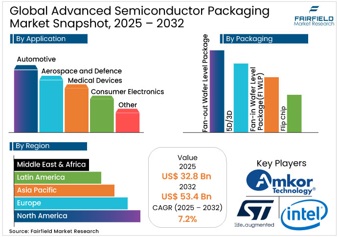
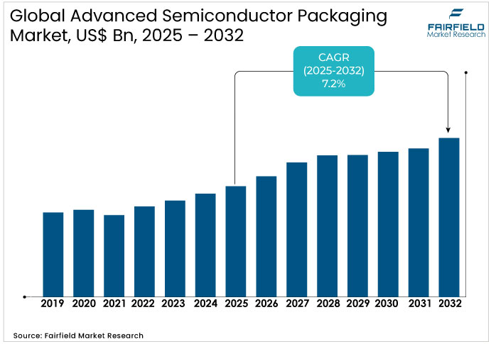
The advanced semiconductor packaging market is valued at USD 32.8 billion in 2025 and is projected to reach USD 53.4 billion by 2032, growing at a CAGR of 7.2%.

Advanced Semiconductor Packaging Market Summary: Key Insights & Trends
- Flip Chip leads the market with ~35% share, dominating logic IC and mobile processor integration.
- 5D/3D packaging records the fastest growth, driven by AI and HPC adoption.
- Consumer Electronics hold ~50% share, supported by strong demand for smartphones and wearables.
- Automotive emerges as the fastest-growing segment with rising EV and ADAS integration.
- AI and HPC advancements accelerate the adoption of multi-die and chiplet-based architectures.
- Fan-out WLP gains momentum from 5G and IoT expansion across smart devices.
- Asia Pacific commands ~65% global share, led by China, Japan, and South Korea.
- North America and Europe strengthen market presence through R&D and supportive semiconductor policies.
Key Growth Drivers
- Miniaturization Drives Breakthroughs in Advanced Semiconductor Packaging
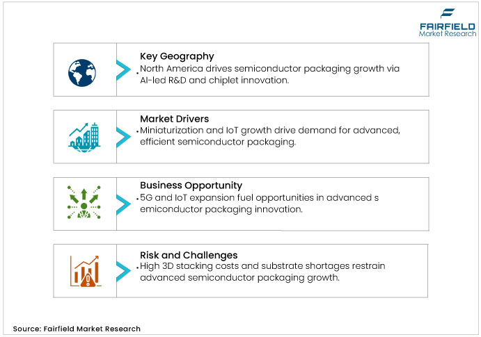
The Advanced Semiconductor Packaging Market thrives as manufacturers prioritize miniaturization to meet consumer needs for compact electronics such as smartphones and wearables. Flip-chip and fan-out technologies enable denser integration, reducing device size while enhancing electrical performance and thermal management. This driver stems from the proliferation of IoT devices, where advanced packaging supports seamless connectivity and energy efficiency. Industry experts note that heterogeneous integration in packaging platforms improves signal integrity and lowers power consumption, justifying investments in R&D. For instance, the global push for 5G networks demands packaging solutions that handle high-frequency signals without degradation. Government agencies report that semiconductor R&D expenditures reached $62.7 billion in 2024, fueling innovations in packaging to address these demands. Justifications include cost optimization through wafer-level processes, which cut manufacturing time and material waste.
- AI Revolution Spurs Multi-Die Integration and 3D Packaging Adoption
AI applications drive the market by requiring multi-die integration for faster data processing and reduced latency. 2.5D/3D packaging allows stacking of logic and memory chips, optimizing performance in data centers and edge computing. Theoretical frameworks highlight how chiplet architectures enable modular designs, facilitating customization for AI workloads without redesigning entire chips. Justifications arise from the need for thermal dissipation in high-density packages, preventing overheating in HPC environments. Associations indicate that AI is projected to contribute over US$15 trillion to the global economy by 2030, underscoring packaging's role in enabling this impact. Furthermore, packaging innovations support quantum computing explorations, where theory focuses on interconnect reliability. This driver encourages collaboration between foundries and OSATs, enhancing competitive edges through patented technologies.

Key Restraints
- Rising Production Costs and Design Complexity Hinder Advanced Semiconductor Packaging Growth
The Advanced Semiconductor Packaging industry faces restraints from elevated costs in designing and producing sophisticated solutions such as 3D stacking, which require specialized equipment and materials. Theory highlights challenges in heat management and signal integrity, increasing development timelines and expenses. Justifications include supply chain vulnerabilities, such as shortages of substrates, limiting scalability in cost-sensitive sectors. Industry analysis note that capital-intensive processes can deter small players, consolidating market power among major firms.
- Evolving Technologies and Stringent Regulations Restrict Long-Term Stability in Semiconductor Packaging
Technological advancements render packaging solutions obsolete quickly, restraining the Advanced Semiconductor Packaging Market as firms struggle to keep pace with evolving standards. Theory emphasizes the risk of short product lifecycles, complicating ROI calculations. Justifications stem from stringent regulations on materials, such as halogen-free requirements, adding compliance burdens. Furthermore, geopolitical tensions disrupt global supply chains, heightening uncertainty for international operations.
Advanced Semiconductor Packaging Market Trends and Opportunities
- 5G and IoT Integration Create Expansive Opportunities in Advanced Semiconductor Packaging
The Advanced Semiconductor Packaging Market unlocks opportunities through 5G and IoT adoption, where fan-out technologies support high-bandwidth components for seamless connectivity. Theory focuses on wafer-level integration to enable edge devices with low power consumption. Justifications include expanding smart cities and industrial automation, demanding scalable packaging for sensors and modules. Opportunities arise from partnerships with telecom giants, theoretically enhancing ecosystem interoperability. Government initiatives, such as subsidies for 5G infrastructure, amplify growth potential.
- Sustainability and Healthcare Innovations Drive Next-Wave Opportunities in Semiconductor Packaging
Sustainability trends offer opportunities as eco-friendly materials gain traction in medical devices and renewable energy. Theory underscores embedded packaging for biocompatible implants, improving patient outcomes through miniaturization. Justifications encompass regulatory emphasis on ESG compliance, driving demand for energy-efficient solutions. Healthcare's shift to wearables requires robust packaging for reliability in vital monitoring. This opportunity encourages R&D in recyclable substrates, theoretically reducing environmental footprints while expanding market reach.

Segment-wise Trends & Analysis
- Flip Chip Leads While 2.5D/3D Packaging Gains Rapid Industry Momentum
Flip Chip holds current market leadership in the Advanced Semiconductor Packaging Market, commanding ~35% share in 2025 due to its superior electrical performance and cost-effectiveness in high-volume production. This dominance stems from widespread adoption in logic ICs and memory devices, where direct chip attachment minimizes interconnect lengths. Competitive positioning favors established players with patented flip-chip processes, enabling them to capture premium segments such as mobile processors.
The growth trajectory for 2.5D/3D packaging emerges as fast-growing in the market, driven by demands for heterogeneous integration in AI and HPC. Underlying drivers include improved thermal management and bandwidth, theoretically allowing modular chiplets for customizable performance. Competitive positioning shifts toward foundries investing in through-silicon vias, positioning them to challenge traditional leaders by offering scalable solutions.
- Consumer Electronics Dominate as Automotive Applications Drive Future Packaging Growth
Consumer Electronics leads with ~50% share in 2025, fueled by demand for feature-rich gadgets such as smartphones and smart home appliances. This leadership reflects packaging's role in enabling high-resolution displays and efficient power distribution. Competitive positioning strengthens for suppliers specializing in miniaturization, securing contracts with major device manufacturers.
Automotive emerges as a fast-growing segment in the Advanced Semiconductor Packaging Sector, propelled by EV adoption and ADAS requirements. Underlying drivers encompass reliability in harsh environments, theoretically supporting sensor fusion for autonomous features. Competitive positioning benefits innovators in power electronics packaging, allowing them to gain ground through collaborations with auto OEMs.
Regional Trends & Analysis
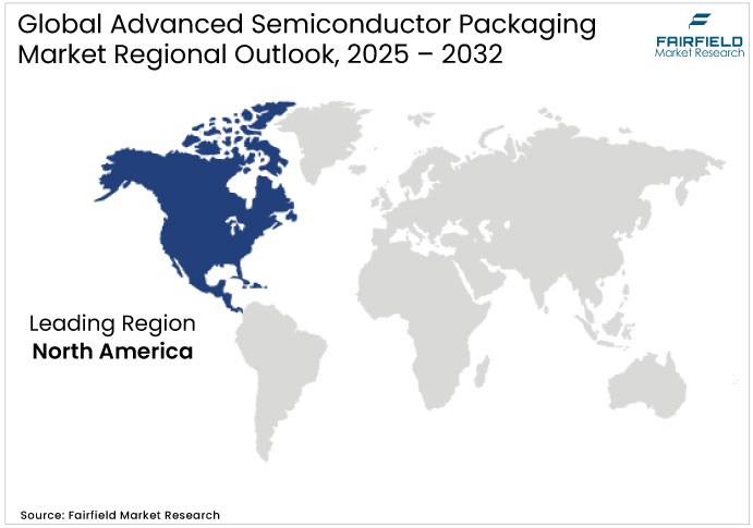
North America Accelerates Semiconductor Packaging Growth with R&D and AI Advancements
North America positions itself as a fast-growing region in the Advanced Semiconductor Packaging Market, with the U.S. spearheading advancements through R&D and AI applications. Trends emphasize heterogeneous integration for data centers, driven by investments in sustainable transportation. The region's ecosystem benefits from collaborations between IDMs and OSATs, fostering innovation in chiplet architectures.

U.S. Advanced Semiconductor Packaging Market - 2025 Snapshot & Outlook
Top trends in the U.S. market include rising EV adoption, necessitating robust packaging for power electronics and ADAS. Drivers involve government policies such as the CHIPS Act, providing $39 billion in grants to expand manufacturing capacity, with exact impact of tripling U.S. chipmaking by 2032. Supportive tax policies, such as the 35% Advanced Manufacturing Investment Credit in 2025, offer margin advantages by reducing costs for R&D facilities. Retail shifts toward AI-enabled devices boost demand, aligning with consumer preferences for efficient electronics.
A consumer trend shows 34.9% of semiconductor demand from computers/AI in 2024, indicating sustained growth in packaging for high-performance applications. Theoretical frameworks highlight supply chain resiliency, mitigating risks through localized production. Overall, the U.S. market's outlook remains optimistic, with policy support enabling competitive edges.
Asia Pacific Dominates Semiconductor Packaging Through 5G and High-Volume Production
Asia Pacific dominates by holding ~65% share in 2025, led by Japan, South Korea, and China as semiconductor hubs. Trends focus on 5G and consumer electronics, with government initiatives such as China's self-sufficiency targets driving innovation. The region excels in high-volume production, theoretically optimizing costs through scale.
Japan Advanced Semiconductor Packaging Market - 2025 Snapshot & Outlook
Top trends in Japan's market revolve around ADAS and autonomous driving, integrating flip-chip for sensors and processors. Drivers include government policies promoting automotive tech, with tax incentives enhancing margin advantages for exporters. Retail shifts to smart vehicles amplify demand, supported by exact impacts from R&D investments.
A consumer trend reveals preference for feature-rich electronics, as per regulator data showing communications end-use at 33.0% globally in 2024. Theoretical emphasis on reliability strengthens positioning against vibrations. The outlook favors continued leadership in precision packaging.
India Advanced Semiconductor Packaging Market - 2025 Snapshot & Outlook
Top trends in India's market include post-COVID incentives for semiconductor manufacturing, boosting AI and IoT applications. Drivers encompass supportive tax policies under PLI schemes, offering margin advantages with exact impacts such as US$10 billion incentives in 2021. Retail shifts toward affordable gadgets drive demand.
A consumer trend from surveys indicates growing adoption of smart homes, with industry association reports noting industrial applications at 8.4% in 2024. Theoretical frameworks prioritize workforce development for scalability. The market's outlook promises emergence as a key player.
Europe Advances Semiconductor Packaging with Focus on Automotive and Automation Technologies
Europe continues to strengthen its foothold in the semiconductor packaging landscape, driven by rising demand from the automotive and industrial automation sectors. Germany and the U.K. remain at the forefront, fostering innovation in sustainable and energy-efficient technologies. The region’s focus on electrification, autonomous vehicles, and Industry 4.0 integration is accelerating adoption of advanced packaging solutions that enable high performance and reliability. Additionally, supportive EU policies and initiatives—such as the European Chips Act—are enhancing cross-border collaboration, research funding, and local manufacturing capabilities, positioning Europe as a critical hub for advanced semiconductor packaging innovation.
Germany Advanced Semiconductor Packaging Market - 2025 Snapshot & Outlook
Top trends in Germany's market center on automotive electronics, integrating 3D packaging for EVs. Drivers include EU Chips Act grants of US$47 billion, providing margin advantages via exact impacts on R&D. Supportive tax policies accelerate adoption.
A consumer trend shows automotive demand at 12.7% globally in 2024. Theoretical focus on durability supports long-term growth. Outlook remains strong for precision applications.
U.K. Advanced Semiconductor Packaging Market - 2025 Snapshot & Outlook
The U.K. advanced semiconductor packaging market in 2025 is witnessing steady growth, supported by expanding automotive electronics, industrial automation, and defense applications. Government-backed initiatives, such as the National Semiconductor Strategy, coupled with strong R&D capabilities and collaborations with global foundries, are driving innovation in high-performance, energy-efficient, and sustainable packaging solutions.
Competitive Landscape
Key Companies
- Intel Corporation
- Amkor Technology
- STMicroelectronics N.V.
- Advanced Semiconductor Engineering, Inc. (ASE) Group
- Advanced Micro Devices, Inc. (AMD)
- Hitachi Chemical
- Infineon
- Avery Dennison
- Sumitomo Chemical
- Kyocera
- China Wafer Level CSP
- Others
Recent Developments:
- June 2025, At the IEEE ECTC, Intel introduced next-gen chip-packaging technologies enabling processors over 21,000 mm² in size—a breakthrough for large AI chips. The innovations enhance die-to-die interconnects (3D EMIB), bonding accuracy, and heat-dissipation systems, allowing integration of 10,000+ mm² of silicon per package to overcome Moore’s Law limits.
- October 2025, Amkor Technology announced a $7 billion expansion of its advanced semiconductor packaging and test campus in Arizona, marking the first U.S.-based high-volume packaging facility. Supported by the CHIPS for America Program and partners such as Apple, NVIDIA, and TSMC, the project will create 3,000 jobs and establish Arizona as a key hub for AI, HPC, and automotive chip manufacturing by 2028.
- April 2025, STMicroelectronics introduced the STM32N6 microcontroller, its most powerful MCU featuring the Neural-ART Accelerator™ NPU that delivers 600× faster AI performance for edge applications. The chip enables advanced computer vision, audio, and sensor analytics in compact, energy-efficient devices, with early adopters such as LG, Lenovo, and Alps Alpine praising its AI capabilities.
Global Advanced Semiconductor Packaging Market Segmentation
By Packaging Type
- Fan-out Wafer Level Package (FO WLP)
- 5D/3D
- Fan-in Wafer Level Package (FI WLP)
- Flip Chip
By Application
- Automotive
- Aerospace and Defence
- Medical Devices
- Consumer Electronics
- Other
By Region
- North America
- Europe
- Asia Pacific
- Latin America
- Middle East & Africa
1. Executive Summary
1.1. Global Advanced Semiconductor Packaging Market Snapshot
1.2. Future Projections
1.3. Key Market Trends
1.4. Regional Snapshot, by Value, 2025
1.5. Analyst Recommendations
2. Market Overview
2.1. Market Definitions and Segmentations
2.2. Market Dynamics
2.2.1. Drivers
2.2.2. Restraints
2.2.3. Market Opportunities
2.3. Value Chain Analysis
2.4. Porter’s Five Forces Analysis
2.5. Covid-19 Impact Analysis
2.5.1. Supply
2.5.2. Demand
2.6. Impact of Ukraine-Russia Conflict
2.7. Economic Overview
2.7.1. World Economic Projections
2.8. PESTLE Analysis
3. Global Advanced Semiconductor Packaging Market Outlook, 2019 - 2032
3.1. Global Advanced Semiconductor Packaging Market Outlook, by Packaging Type, Value (US$ Bn), 2019 - 2032
3.1.1. Key Highlights
3.1.1.1. FO WLP
3.1.1.2. 2.5D/3D
3.1.1.3. FI WLP
3.1.1.4. Flip Chip
3.2. Global Advanced Semiconductor Packaging Market Outlook, by Application, Value (US$ Bn), 2019 - 2032
3.2.1. Key Highlights
3.2.1.1. Automotive
3.2.1.2. Aerospace and Defense
3.2.1.3. Medical Devices
3.2.1.4. Consumer Electronics
3.2.1.5. Other
3.3. Global Advanced Semiconductor Packaging Market Outlook, by Region, Value (US$ Bn), 2019 - 2032
3.3.1. Key Highlights
3.3.1.1. North America
3.3.1.2. Europe
3.3.1.3. Asia Pacific
3.3.1.4. Latin America
3.3.1.5. Middle East & Africa
4. North America Advanced Semiconductor Packaging Market Outlook, 2019 - 2032
4.1. North America Advanced Semiconductor Packaging Market Outlook, by Packaging Type, Value (US$ Bn), 2019 - 2032
4.1.1. Key Highlights
4.1.1.1. FO WLP
4.1.1.2. 2.5D/3D
4.1.1.3. FI WLP
4.1.1.4. Flip Chip
4.2. North America Advanced Semiconductor Packaging Market Outlook, by Application, Value (US$ Bn), 2019 - 2032
4.2.1. Key Highlights
4.2.1.1. Automotive
4.2.1.2. Aerospace and Defense
4.2.1.3. Medical Devices
4.2.1.4. Consumer Electronics
4.2.1.5. Other
4.2.2. Market Attractiveness Analysis
4.3. North America Advanced Semiconductor Packaging Market Outlook, by Country, Value (US$ Bn), 2019 - 2032
4.3.1. Key Highlights
4.3.1.1. U.S. Advanced Semiconductor Packaging Market by Packaging Type, Value (US$ Bn), 2019 - 2032
4.3.1.2. U.S. Advanced Semiconductor Packaging Market Application, Value (US$ Bn), 2019 - 2032
4.3.1.3. Canada Advanced Semiconductor Packaging Market by Packaging Type, Value (US$ Bn), 2019 - 2032
4.3.1.4. Canada Advanced Semiconductor Packaging Market Application, Value (US$ Bn), 2019 - 2032
4.3.2. BPS Analysis/Market Attractiveness Analysis
5. Europe Advanced Semiconductor Packaging Market Outlook, 2019 - 2032
5.1. Europe Advanced Semiconductor Packaging Market Outlook, by Packaging Type, Value (US$ Bn), 2019 - 2032
5.1.1. Key Highlights
5.1.1.1. FO WLP
5.1.1.2. 2.5D/3D
5.1.1.3. FI WLP
5.1.1.4. Flip Chip
5.2. Europe Advanced Semiconductor Packaging Market Outlook, by Application, Value (US$ Bn), 2019 - 2032
5.2.1. Key Highlights
5.2.1.1. Automotive
5.2.1.2. Aerospace and Defense
5.2.1.3. Medical Devices
5.2.1.4. Consumer Electronics
5.2.1.5. Other
5.2.2. BPS Analysis/Market Attractiveness Analysis
5.3. Europe Advanced Semiconductor Packaging Market Outlook, by Country, Value (US$ Bn), 2019 - 2032
5.3.1. Key Highlights
5.3.1.1. Germany Advanced Semiconductor Packaging Market by Packaging Type, Value (US$ Bn), 2019 - 2032
5.3.1.2. Germany Advanced Semiconductor Packaging Market Application, Value (US$ Bn), 2019 - 2032
5.3.1.3. U.K. Advanced Semiconductor Packaging Market by Packaging Type, Value (US$ Bn), 2019 - 2032
5.3.1.4. U.K. Advanced Semiconductor Packaging Market Application, Value (US$ Bn), 2019 - 2032
5.3.1.5. France Advanced Semiconductor Packaging Market by Packaging Type, Value (US$ Bn), 2019 - 2032
5.3.1.6. France Advanced Semiconductor Packaging Market Application, Value (US$ Bn), 2019 - 2032
5.3.1.7. Italy Advanced Semiconductor Packaging Market by Packaging Type, Value (US$ Bn), 2019 - 2032
5.3.1.8. Italy Advanced Semiconductor Packaging Market Application, Value (US$ Bn), 2019 - 2032
5.3.1.9. Spain Advanced Semiconductor Packaging Market by Packaging Type, Value (US$ Bn), 2019 - 2032
5.3.1.10. Spain Advanced Semiconductor Packaging Market Application, Value (US$ Bn), 2019 - 2032
5.3.1.11. Spain Advanced Semiconductor Packaging Market by Packaging Type, Value (US$ Bn), 2019 - 2032
5.3.1.12. Russia Advanced Semiconductor Packaging Market Application, Value (US$ Bn), 2019 - 2032
5.3.1.13. Rest of Europe Advanced Semiconductor Packaging Market by Packaging Type, Value (US$ Bn), 2019 - 2032
5.3.1.14. Rest of Europe Advanced Semiconductor Packaging Market Application, Value (US$ Bn), 2019 - 2032
5.3.2. BPS Analysis/Market Attractiveness Analysis
6. Asia Pacific Advanced Semiconductor Packaging Market Outlook, 2019 - 2032
6.1. Asia Pacific Advanced Semiconductor Packaging Market Outlook, by Packaging Type, Value (US$ Bn), 2019 - 2032
6.1.1. Key Highlights
6.1.1.1. FO WLP
6.1.1.2. 2.5D/3D
6.1.1.3. FI WLP
6.1.1.4. Flip Chip
6.2. Asia Pacific Advanced Semiconductor Packaging Market Outlook, by Application, Value (US$ Bn), 2019 - 2032
6.2.1. Key Highlights
6.2.1.1. Automotive
6.2.1.2. Aerospace and Defense
6.2.1.3. Medical Devices
6.2.1.4. Consumer Electronics
6.2.1.5. Other
6.2.2. BPS Analysis/Market Attractiveness Analysis
6.3. Asia Pacific Advanced Semiconductor Packaging Market Outlook, by Country, Value (US$ Bn), 2019 - 2032
6.3.1. Key Highlights
6.3.1.1. China Advanced Semiconductor Packaging Market by Packaging Type, Value (US$ Bn), 2019 - 2032
6.3.1.2. China Advanced Semiconductor Packaging Market Application, Value (US$ Bn), 2019 - 2032
6.3.1.3. Japan Advanced Semiconductor Packaging Market by Packaging Type, Value (US$ Bn), 2019 - 2032
6.3.1.4. Japan Advanced Semiconductor Packaging Market Application, Value (US$ Bn), 2019 - 2032
6.3.1.5. South Korea Advanced Semiconductor Packaging Market by Packaging Type, Value (US$ Bn), 2019 - 2032
6.3.1.6. South Korea Advanced Semiconductor Packaging Market Application, Value (US$ Bn), 2019 - 2032
6.3.1.7. India Advanced Semiconductor Packaging Market by Packaging Type, Value (US$ Bn), 2019 - 2032
6.3.1.8. India Advanced Semiconductor Packaging Market Application, Value (US$ Bn), 2019 - 2032
6.3.1.9. Southeast Asia Advanced Semiconductor Packaging Market by Packaging Type, Value (US$ Bn), 2019 - 2032
6.3.1.10. Southeast Asia Advanced Semiconductor Packaging Market Application, Value (US$ Bn), 2019 - 2032
6.3.1.11. Rest of Asia Pacific Advanced Semiconductor Packaging Market by Packaging Type, Value (US$ Bn), 2019 - 2032
6.3.1.12. Rest of Asia Pacific Advanced Semiconductor Packaging Market Application, Value (US$ Bn), 2019 - 2032
6.3.2. BPS Analysis/Market Attractiveness Analysis
7. Latin America Advanced Semiconductor Packaging Market Outlook, 2019 - 2032
7.1. Latin America Advanced Semiconductor Packaging Market Outlook, by Packaging Type, Value (US$ Bn), 2019 - 2032
7.1.1. Key Highlights
7.1.1.1. FO WLP
7.1.1.2. 2.5D/3D
7.1.1.3. FI WLP
7.1.1.4. Flip Chip
7.2. Latin America Advanced Semiconductor Packaging Market Outlook, by Application, Value (US$ Bn), 2019 - 2032
7.2.1. Key Highlights
7.2.1.1. Automotive
7.2.1.2. Aerospace and Defense
7.2.1.3. Medical Devices
7.2.1.4. Consumer Electronics
7.2.1.5. Other
7.2.2. BPS Analysis/Market Attractiveness Analysis
7.3. Latin America Advanced Semiconductor Packaging Market Outlook, by Country, Value (US$ Bn), 2019 - 2032
7.3.1. Key Highlights
7.3.1.1. Brazil Advanced Semiconductor Packaging Market by Packaging Type, Value (US$ Bn), 2019 - 2032
7.3.1.2. Brazil Advanced Semiconductor Packaging Market Application, Value (US$ Bn), 2019 - 2032
7.3.1.3. Mexico Advanced Semiconductor Packaging Market by Packaging Type, Value (US$ Bn), 2019 - 2032
7.3.1.4. Mexico Advanced Semiconductor Packaging Market Application, Value (US$ Bn), 2019 - 2032
7.3.1.5. Rest of Latin America Advanced Semiconductor Packaging Market by Packaging Type, Value (US$ Bn), 2019 - 2032
7.3.1.6. Rest of Latin America Advanced Semiconductor Packaging Market Application, Value (US$ Bn), 2019 - 2032
7.3.2. BPS Analysis/Market Attractiveness Analysis
8. Middle East & Africa Advanced Semiconductor Packaging Market Outlook, 2019 - 2032
8.1. Middle East & Africa Advanced Semiconductor Packaging Market Outlook, by Packaging Type, Value (US$ Bn), 2019 - 2032
8.1.1. Key Highlights
8.1.1.1. FO WLP
8.1.1.2. 2.5D/3D
8.1.1.3. FI WLP
8.1.1.4. Flip Chip
8.2. Middle East & Africa Advanced Semiconductor Packaging Market Outlook, by Application, Value (US$ Bn), 2019 - 2032
8.2.1. Key Highlights
8.2.1.1. Automotive
8.2.1.2. Aerospace and Defense
8.2.1.3. Medical Devices
8.2.1.4. Consumer Electronics
8.2.1.5. Other
8.2.2. BPS Analysis/Market Attractiveness Analysis
8.3. Middle East & Africa Advanced Semiconductor Packaging Market Outlook, by Country, Value (US$ Bn), 2019 - 2032
8.3.1. Key Highlights
8.3.1.1. GCC Advanced Semiconductor Packaging Market by Packaging Type, Value (US$ Bn), 2019 - 2032
8.3.1.2. GCC Advanced Semiconductor Packaging Market Application, Value (US$ Bn), 2019 - 2032
8.3.1.3. South Africa Advanced Semiconductor Packaging Market by Packaging Type, Value (US$ Bn), 2019 - 2032
8.3.1.4. South Africa Advanced Semiconductor Packaging Market Application, Value (US$ Bn), 2019 - 2032
8.3.1.5. Rest of Middle East & Africa Advanced Semiconductor Packaging Market by Packaging Type, Value (US$ Bn), 2019 - 2032
8.3.1.6. Rest of Middle East & Africa Advanced Semiconductor Packaging Market Application, Value (US$ Bn), 2019 - 2032
8.3.2. BPS Analysis/Market Attractiveness Analysis
9. Competitive Landscape
9.1. Manufacturer vs Packaging Type Heatmap
9.2. Company Market Share Analysis, 2024
9.3. Competitive Dashboard
9.4. Company Profiles
9.4.1. Advanced Semiconductor Engineering, Inc.
9.4.1.1. Company Overview
9.4.1.2. Product Portfolio
9.4.1.3. Financial Overview
9.4.1.4. Business Strategies and Development
9.4.2. Advanced Micro Devices, Inc. (AMD)
9.4.2.1. Company Overview
9.4.2.2. Product Portfolio
9.4.2.3. Financial Overview
9.4.2.4. Business Strategies and Development
9.4.3. Intel Corporation
9.4.3.1. Company Overview
9.4.3.2. Product Portfolio
9.4.3.3. Financial Overview
9.4.3.4. Business Strategies and Development
9.4.4. Amkor Technology
9.4.4.1. Company Overview
9.4.4.2. Product Portfolio
9.4.4.3. Financial Overview
9.4.4.4. Business Strategies and Development
9.4.5. STMicroelectronics N.V.
9.4.5.1. Company Overview
9.4.5.2. Product Portfolio
9.4.5.3. Financial Overview
9.4.5.4. Business Strategies and Development
9.4.6. Hitachi Chemical
9.4.6.1. Company Overview
9.4.6.2. Product Portfolio
9.4.6.3. Financial Overview
9.4.6.4. Business Strategies and Development
9.4.7. Infineon
9.4.7.1. Company Overview
9.4.7.2. Product Portfolio
9.4.7.3. Financial Overview
9.4.7.4. Business Strategies and Development
9.4.8. Avery Dennison
9.4.8.1. Company Overview
9.4.8.2. Product Portfolio
9.4.8.3. Financial Overview
9.4.8.4. Business Strategies and Development
9.4.9. Sumitomo Chemical
9.4.9.1. Company Overview
9.4.9.2. Product Portfolio
9.4.9.3. Business Strategies and Development
9.4.10. ASE Group
9.4.10.1. Company Overview
9.4.10.2. Product Portfolio
9.4.10.3. Financial Overview
9.4.10.4. Business Strategies and Development
9.4.11. Kyocera
9.4.11.1. Company Overview
9.4.11.2. Product Portfolio
9.4.11.3. Financial Overview
9.4.11.4. Business Strategies and Development
9.4.12. China Wafer Level CSP
9.4.12.1. Company Overview
9.4.12.2. Product Portfolio
9.4.12.3. Financial Overview
9.4.12.4. Business Strategies and Development
10. Appendix
10.1. Research Methodology
10.2. Report Assumptions
10.3. Acronyms and Abbreviations
|
BASE YEAR |
HISTORICAL DATA |
FORECAST PERIOD |
UNITS |
|||
|
2024 |
|
2019 - 2024 |
2025 - 2032 |
Value: US$ Bn Volume: Kilo Tons |
||
|
REPORT FEATURES |
DETAILS |
|
Packaging Type Coverage |
|
|
Application Coverage |
|
|
Geographical Coverage |
|
|
Leading Companies |
|
|
Report Highlights |
Market Estimates and Forecast, Market Dynamics, Industry Trends, Production Output, Trade Statistics, Price Trend Analysis, Competition Landscape, Grade-, Application-, Region-, Country-wise Trends & Analysis, COVID-19 Impact Analysis (Demand and Supply), Key Market Trends |
