



Electrostatic Chucks (ESCs) Market
Electrostatic Chucks (ESCs) Market Insights, Competitive Landscape, and Market Forecast - 2033
Global Electrostatic Chucks (ESCs) Market Forecast
- The Electrostatic Chucks (ESCs) Market is expected to grow from USD 2 Billion in 2026 to USD 3.3 Billion by 2033, reflecting strong industry expansion and registering a CAGR of 7.6% during the forecast period from 2026 to 2033.
- The Electrostatic Chucks (ESCs) market is anticipated to benefit from strong demand due to the increasing need for precision and stability, particularly in wafer handling and processing.
Electrostatic Chucks (ESCs) Market Insights
- The growing demand for advanced semiconductor devices, including chips for AI, automotive, and 5G technology, has significantly increased the adoption.
- Ceramic materials are expected to dominate the ESCs market with an 89.1% share in 2025. This dominance is attributed to their superior electrical insulation properties and exceptional thermal stability, making them ideal for high-precision applications.
- The trend towards miniaturization of electronic devices, particularly in the mobile, wearable, and IoT sectors, drives the need for precise wafer handling solutions.
- Gaining traction in flat panel display manufacturing, where precise alignment and handling of thin substrates are crucial for the production of high-resolution displays.
- The rise of automation and smart manufacturing processes is contributing to the increased need for advanced ESCs that can integrate with robotic systems and other automated equipment.
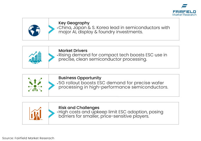
- Asia Pacific leads the market, fueled by the rapid growth of semiconductor manufacturing. The region's investments in advanced manufacturing technologies and demand for high-precision processes, including semiconductor fabrication and flat-panel display production, drive its market dominance.
- Electrostatic chucks are increasingly integrated with Internet of Things (IoT) technology, enabling real-time monitoring and control of wafer temperature, pressure, and positioning during manufacturing processes.
A Look Back and a Look Forward - Comparative Analysis
The historical growth of the Electrostatic Chucks market has been primarily driven by the rising demand from the semiconductor and flat panel display industries. The increasing complexity and miniaturization of semiconductor devices pushed the adoption of advanced wafer handling solutions. Despite disruptions in 2020 due to global supply chain constraints and manufacturing halts, the market rebounded swiftly in 2021 as chip shortages highlighted the need for capacity expansion. Innovations in materials and better integration with vacuum and cooling systems further supported product development and deployment.
Looking ahead, the Electrostatic Chucks market is expected to advance significantly due to ongoing technological innovation and the expansion of advanced node semiconductor fabrication. The rising deployment of EUV lithography and the continued scaling of chip architectures drives the demand for more reliable and stable wafer clamping solutions. Emerging applications such as quantum computing, photonics, and advanced displays are likely to increase the need for high-precision wafer processing. Environmental concerns and energy efficiency goals are expected to lead to design enhancements that reduce power consumption and improve thermal control.
Key Growth Determinants
- Miniaturization of Electronic Devices Driving ESC Market Growth
The growing demand for smaller, more efficient, and multifunctional gadgets has increased the need for advanced semiconductor manufacturing processes, with electrostatic chucks (ESCs) playing a crucial role in ensuring precision, stability, and cleanliness during wafer fabrication. As transistors shrink and integrated circuits (ICs) become more complex, ESCs have become indispensable in modern semiconductor processing. They provide superior wafer clamping with minimal contamination risk, enabling precise positioning and uniform thermal control, which is critical for handling small geometries in miniaturized components.
Miniaturization has also led to the use of advanced wafer sizes and thinner substrates, placing additional stress on traditional mechanical clamping methods that can damage fragile wafers. For instance, South Korea plans to build the world’s largest semiconductor cluster in Gyeonggi Province by investing approximately $470 billion (€430 billion) over the next 23 years into the massive production park in partnership with major electronics companies such as Samsung Electronics and SK Hynix. South Korea projects to increase its self-sufficiency in essential materials, parts, and equipment for chip production to 50% by 2030.
Key Growth Barriers
- Technical Complexity and Cost
The high initial investment required for acquiring and implementing these systems poses a significant barrier to market penetration. These systems involve complex designs and precise manufacturing processes, which drive up production costs, ultimately passed on to end-users. Periodic maintenance, recalibration, and potential upgrades further increase the total cost of ownership, making it difficult for price-sensitive industries to justify the expense. The competitive landscape, with larger players benefiting from economies of scale, makes it challenging for smaller companies to compete in price, limiting market entry and growth.
These systems rely on electrostatic attraction to securely hold substrates during manufacturing, but certain materials or surface coatings do not exhibit optimal electrostatic properties, complicating reliable clamping. Customized electrostatic chuck solutions are often required for non-standard substrates or processes, making them time-consuming and costly to develop. For example, variation in substrate size, shape, or surface roughness limits the scalability and flexibility of electrostatic chuck applications, particularly in niche or emerging technologies like advanced semiconductor fabrication for 3D NAND memory or OLED panels.
Electrostatic Chucks Market Trends and Opportunities
- Expansion of 5G and AI Technology
With the need for faster and more powerful communication infrastructure, the production of high-performance semiconductors for 5G base stations and mobile devices is crucial. ESCs play a vital role in wafer processing, ensuring secure and stable positioning during critical processes such as photolithography and etching, which are essential for the required accuracy in 5G components. As of October 2024, over 4 lakh 5G base transceiver stations (BTSs) have been installed in India, emphasizing the growing need for precision in semiconductor fabrication.
The expansion of AI applications across various industries, such as robotics, machine learning, and data centers, further boosts the demand for high-performance chips. These chips require intricate semiconductor fabrication, where ESCs provide the necessary precision for wafer handling. With AI adoption accelerating, particularly in sectors like healthcare, automotive, and consumer electronics, the demand for advanced chips grows. For instance, IndiaAI Mission's funding of ₹2,000 crore for FY2025-26 aims to enhance AI capabilities, including the development of advanced chips that rely on precise manufacturing.
- Development of Multi-zone and Bipolar ESCs
The growing demand for finer semiconductor geometries and higher-performance chips is driving the adoption of advanced ESC designs, such as multi-zone and bipolar configurations. Multi-zone ESCs offer localized clamping across different chuck surface areas, improving thermal contact and process consistency, especially with warped or uneven wafers. In 300mm wafer processing, they enable precise control of individual zones to maintain uniform temperature and pressure, ensuring high yield during etching or deposition.
Bipolar ESCs, which use dual polarity electrodes, provide stronger clamping at lower voltages, improving safety and reducing energy use. Their superior performance in high-temperature environments makes them well-suited for plasma etching and advanced chip fabrication. As heterogeneous integration gains traction, the flexibility of multi-zone ESCs supports non-standard substrates in 2.5D/3D packaging. For instance, in 2022, the CHIPS and Science Act in the U.S. allocated $53 billion to enhance semiconductor research and manufacturing.
By 2024, the Commerce Department announced over $30 billion in CHIPS private sector investments across 23 projects, including 16 new semiconductor plants, expected to create over 115,000 jobs. Such investments are expected to enhance the adoption of advanced manufacturing equipment, including multi-zone and bipolar ESCs, to meet the growing demand for semiconductors.
Leading Segment Overview
- Coulomb ESCs Ensure High Accuracy and Yield in Integrated Circuit Production
Coulomb ESCs are expected to account for 69.8% share in 2025, due to their superior performance in precision handling and stability. These ESCs use electrostatic forces to securely hold semiconductor wafers during manufacturing processes, ensuring minimal damage and high accuracy. Their ability to provide uniform clamping forces across the wafer surface is particularly beneficial in applications like semiconductor fabrication, where tight tolerances are critical. It offers reliable control over wafer positioning, contributing to better process control and yield rates.
For example, in the production of integrated circuits, Coulomb ESCs are widely used to maintain precise wafer alignment during photolithography or etching, helping to achieve high-quality output with minimal defects. These factors make them the preferred choice for many advanced manufacturing applications.
Johnsen-Rahbek (JR) ESCs offer enhanced clamping force uniformity and wafer stability, making them ideal for critical semiconductor processes like advanced lithography and metrology. Their superior performance in ultra-precise applications positions them for sustained growth in niche markets, driven by the increasing demand for next-generation semiconductor devices.
- Ceramic Materials Leading the Way in Enhancing Durability and Precision in Wafer Processing
Ceramic is expected to hold 89.1% revenue share of the electrostatic chuck market in 2025, driven by its superior electrical insulation properties, thermal stability, and robustness in harsh environments. They are ideal for high-precision applications because they offer excellent heat dissipation and withstand extreme temperatures during wafer processing. For example, materials such as alumina and zirconia are commonly used in ceramic ESCs, providing enhanced durability and reliability. Ceramics are non-reactive, preventing chemical interaction with wafers, thereby reducing the risk of contamination. Their ability to maintain stable electrical characteristics under varying conditions further enhances their reliability and precision.
Regional Analysis
- Asia Pacific is the Largest Market for the Electrostatic Chucks
Major economies such as China, Japan, and South Korea dominate global semiconductor and display panel manufacturing, with substantial investments in AI chips, next-gen memory, and flexible displays. China is strategically boosting self-sufficiency through initiatives such as Made in China 2025 and expanding domestic foundries such as SMIC. China is significantly increasing DUV and legacy node production, driving strong demand for ESCs. In May 2024, China launched the National Integrated Circuit Industry Investment Fund III with a capital of 344 billion yuan ($47.5 billion), supporting large-scale manufacturing and equipment, while Huawei achieved a 40% yield in advanced AI chip production by 2025.
Japan, while no longer a leader in chip foundries, remains a key supplier of semiconductor equipment and materials, particularly in high-performance ceramics and dielectric materials that enhance ESC reliability and functionality. India, under the Make in India initiative, is building its semiconductor ecosystem with projects like the Vedanta-Foxconn JV and Micron’s assembly unit in Gujarat. In 2024, the Indian government approved several semiconductor units under the Semicon India Programme, securing US$ 1.51 billion in investments, driving future demand for ESCs through foreign equipment and eventually domestic production.
- North America's Semiconductor and Tech Advancements
North America is experiencing growth driven by the transition to smaller chip nodes, 3D architectures, and the integration of AI and high-performance computing (HPC) into consumer and defense electronics, requiring advanced-node semiconductors and precise wafer handling. For instance, Samsung’s US$40 billion investment in Texas, including two new fabrication plants and a research facility is supported by a US$4.74 billion U.S. Department of Commerce grant. Additionally, Intel has received approximately US$7.9 billion in federal grants under the CHIPS Act to strengthen its semiconductor manufacturing capabilities.
In Canada, strong R&D efforts in compound semiconductors and MEMS devices by universities and startups are driving the demand for customized solutions. Clean technology and electronics recycling policies also promote ESC use in precision sorting and material recovery. Industries such as medical devices, aerospace, and optics are adopting wafer-level packaging and microfabrication. In July 2024, the Canadian government announced a $120 million investment in the FABrIC network to boost the semiconductor and smart sensor industries while fostering innovation and a skilled workforce.
- Europe’s Demand for Precision Components Driven by Industry 4.0 and Advanced Manufacturing
Germany, with its strong industrial base in precision engineering, automotive, and automation, plays a significant role in driving demand for electrostatic chucks. The country's commitment to Industry 4.0, with a focus on automation, IoT, and smart factories, has further accelerated this demand. For instance, Germany's US$2.2 billion investment to enhance its microelectronics ecosystem aligns with the European Chips Act, aiming to reduce reliance on Asian suppliers and boosting the need for high-precision manufacturing equipment.
The U.K., aiming to establish itself as a technology and manufacturing leader post-Brexit, has increased demand for precision components in sectors like semiconductors, aerospace, and electronics. Its push for semiconductor self-sufficiency highlights the importance of these high-precision tools in modern manufacturing environments. France’s substantial investments in R&D, particularly in defense and civilian aerospace, and Spain’s focus on renewable energy and electronics manufacturing, have led to growing needs for precise components in the production of energy systems and electric vehicle batteries.
Competitive Landscape
• SHINKO ELECTRIC INDUSTRIES CO. LTD.
• TOTO LTD.
• NGK INSULATORS, LTD.
• KYOCERA Corporation
• NTK CERATEC CO., LTD.
• Entegris, Inc.
• CREATIVE TECHNOLOGY CO.
• TOMOEGAWA CO., LTD.
• MiCo Co., Ltd.
• BOBOO Hightech Co., Ltd.
Global Electrostatic Chucks (ESCs) Market is segmented as-
By Technology
• Coulomb ESCs
• Johnsen-Rahbek (JR) ESCs
By Material
• Ceramic
• Quartz
By Application
• Semiconductor Manufacturing
• Flat Panel Display (FPD) Manufacturing
• Medical Device
• Others
By Region
• North America
• Europe
• Asia Pacific
• Latin America
• Middle East & Africa
- Executive Summary
- Global Electrostatic Chucks (ESCs) Market Snapshot
- Future Projections
- Key Market Trends
- Regional Snapshot, by Value, 2026
- Analyst Recommendations
- Market Overview
- Market Definitions and Segmentations
- Market Dynamics
- Drivers
- Restraints
- Market Opportunities
- Value Chain Analysis
- COVID-19 Impact Analysis
- Porter's Five Forces Analysis
- Impact of Russia-Ukraine Conflict
- PESTLE Analysis
- Regulatory Analysis
- Price Trend Analysis
- Current Prices and Future Projections, 2025-2033
- Price Impact Factors
- Global Electrostatic Chucks (ESCs) Market Outlook, 2020 - 2033
- Global Electrostatic Chucks (ESCs) Market Outlook, by Technology, Value (US$ Bn), 2020-2033
- Coulomb ESCs
- Johnsen-Rahbek (JR) ESCs
- Global Electrostatic Chucks (ESCs) Market Outlook, by Material, Value (US$ Bn), 2020-2033
- Ceramic
- Quartz
- Global Electrostatic Chucks (ESCs) Market Outlook, by Application, Value (US$ Bn), 2020-2033
- Semiconductor Manufacturing
- Flat Panel Display (FPD) Manufacturing
- Medical Device
- Global Electrostatic Chucks (ESCs) Market Outlook, by Region, Value (US$ Bn), 2020-2033
- North America
- Europe
- Asia Pacific
- Latin America
- Middle East & Africa
- Global Electrostatic Chucks (ESCs) Market Outlook, by Technology, Value (US$ Bn), 2020-2033
- North America Electrostatic Chucks (ESCs) Market Outlook, 2020 - 2033
- North America Electrostatic Chucks (ESCs) Market Outlook, by Technology, Value (US$ Bn), 2020-2033
- Coulomb ESCs
- Johnsen-Rahbek (JR) ESCs
- North America Electrostatic Chucks (ESCs) Market Outlook, by Material, Value (US$ Bn), 2020-2033
- Ceramic
- Quartz
- North America Electrostatic Chucks (ESCs) Market Outlook, by Application, Value (US$ Bn), 2020-2033
- Semiconductor Manufacturing
- Flat Panel Display (FPD) Manufacturing
- Medical Device
- North America Electrostatic Chucks (ESCs) Market Outlook, by Country, Value (US$ Bn), 2020-2033
- U.S. Electrostatic Chucks (ESCs) Market Outlook, by Technology, 2020-2033
- U.S. Electrostatic Chucks (ESCs) Market Outlook, by Material, 2020-2033
- U.S. Electrostatic Chucks (ESCs) Market Outlook, by Application, 2020-2033
- Canada Electrostatic Chucks (ESCs) Market Outlook, by Technology, 2020-2033
- Canada Electrostatic Chucks (ESCs) Market Outlook, by Material, 2020-2033
- Canada Electrostatic Chucks (ESCs) Market Outlook, by Application, 2020-2033
- BPS Analysis/Market Attractiveness Analysis
- North America Electrostatic Chucks (ESCs) Market Outlook, by Technology, Value (US$ Bn), 2020-2033
- Europe Electrostatic Chucks (ESCs) Market Outlook, 2020 - 2033
- Europe Electrostatic Chucks (ESCs) Market Outlook, by Technology, Value (US$ Bn), 2020-2033
- Coulomb ESCs
- Johnsen-Rahbek (JR) ESCs
- Europe Electrostatic Chucks (ESCs) Market Outlook, by Material, Value (US$ Bn), 2020-2033
- Ceramic
- Quartz
- Europe Electrostatic Chucks (ESCs) Market Outlook, by Application, Value (US$ Bn), 2020-2033
- Semiconductor Manufacturing
- Flat Panel Display (FPD) Manufacturing
- Medical Device
- Europe Electrostatic Chucks (ESCs) Market Outlook, by Country, Value (US$ Bn), 2020-2033
- Germany Electrostatic Chucks (ESCs) Market Outlook, by Technology, 2020-2033
- Germany Electrostatic Chucks (ESCs) Market Outlook, by Material, 2020-2033
- Germany Electrostatic Chucks (ESCs) Market Outlook, by Application, 2020-2033
- Italy Electrostatic Chucks (ESCs) Market Outlook, by Technology, 2020-2033
- Italy Electrostatic Chucks (ESCs) Market Outlook, by Material, 2020-2033
- Italy Electrostatic Chucks (ESCs) Market Outlook, by Application, 2020-2033
- France Electrostatic Chucks (ESCs) Market Outlook, by Technology, 2020-2033
- France Electrostatic Chucks (ESCs) Market Outlook, by Material, 2020-2033
- France Electrostatic Chucks (ESCs) Market Outlook, by Application, 2020-2033
- U.K. Electrostatic Chucks (ESCs) Market Outlook, by Technology, 2020-2033
- U.K. Electrostatic Chucks (ESCs) Market Outlook, by Material, 2020-2033
- U.K. Electrostatic Chucks (ESCs) Market Outlook, by Application, 2020-2033
- Spain Electrostatic Chucks (ESCs) Market Outlook, by Technology, 2020-2033
- Spain Electrostatic Chucks (ESCs) Market Outlook, by Material, 2020-2033
- Spain Electrostatic Chucks (ESCs) Market Outlook, by Application, 2020-2033
- Russia Electrostatic Chucks (ESCs) Market Outlook, by Technology, 2020-2033
- Russia Electrostatic Chucks (ESCs) Market Outlook, by Material, 2020-2033
- Russia Electrostatic Chucks (ESCs) Market Outlook, by Application, 2020-2033
- Rest of Europe Electrostatic Chucks (ESCs) Market Outlook, by Technology, 2020-2033
- Rest of Europe Electrostatic Chucks (ESCs) Market Outlook, by Material, 2020-2033
- Rest of Europe Electrostatic Chucks (ESCs) Market Outlook, by Application, 2020-2033
- BPS Analysis/Market Attractiveness Analysis
- Europe Electrostatic Chucks (ESCs) Market Outlook, by Technology, Value (US$ Bn), 2020-2033
- Asia Pacific Electrostatic Chucks (ESCs) Market Outlook, 2020 - 2033
- Asia Pacific Electrostatic Chucks (ESCs) Market Outlook, by Technology, Value (US$ Bn), 2020-2033
- Coulomb ESCs
- Johnsen-Rahbek (JR) ESCs
- Asia Pacific Electrostatic Chucks (ESCs) Market Outlook, by Material, Value (US$ Bn), 2020-2033
- Ceramic
- Quartz
- Asia Pacific Electrostatic Chucks (ESCs) Market Outlook, by Application, Value (US$ Bn), 2020-2033
- Semiconductor Manufacturing
- Flat Panel Display (FPD) Manufacturing
- Medical Device
- Asia Pacific Electrostatic Chucks (ESCs) Market Outlook, by Country, Value (US$ Bn), 2020-2033
- China Electrostatic Chucks (ESCs) Market Outlook, by Technology, 2020-2033
- China Electrostatic Chucks (ESCs) Market Outlook, by Material, 2020-2033
- China Electrostatic Chucks (ESCs) Market Outlook, by Application, 2020-2033
- Japan Electrostatic Chucks (ESCs) Market Outlook, by Technology, 2020-2033
- Japan Electrostatic Chucks (ESCs) Market Outlook, by Material, 2020-2033
- Japan Electrostatic Chucks (ESCs) Market Outlook, by Application, 2020-2033
- South Korea Electrostatic Chucks (ESCs) Market Outlook, by Technology, 2020-2033
- South Korea Electrostatic Chucks (ESCs) Market Outlook, by Material, 2020-2033
- South Korea Electrostatic Chucks (ESCs) Market Outlook, by Application, 2020-2033
- India Electrostatic Chucks (ESCs) Market Outlook, by Technology, 2020-2033
- India Electrostatic Chucks (ESCs) Market Outlook, by Material, 2020-2033
- India Electrostatic Chucks (ESCs) Market Outlook, by Application, 2020-2033
- Southeast Asia Electrostatic Chucks (ESCs) Market Outlook, by Technology, 2020-2033
- Southeast Asia Electrostatic Chucks (ESCs) Market Outlook, by Material, 2020-2033
- Southeast Asia Electrostatic Chucks (ESCs) Market Outlook, by Application, 2020-2033
- Rest of SAO Electrostatic Chucks (ESCs) Market Outlook, by Technology, 2020-2033
- Rest of SAO Electrostatic Chucks (ESCs) Market Outlook, by Material, 2020-2033
- Rest of SAO Electrostatic Chucks (ESCs) Market Outlook, by Application, 2020-2033
- BPS Analysis/Market Attractiveness Analysis
- Asia Pacific Electrostatic Chucks (ESCs) Market Outlook, by Technology, Value (US$ Bn), 2020-2033
- Latin America Electrostatic Chucks (ESCs) Market Outlook, 2020 - 2033
- Latin America Electrostatic Chucks (ESCs) Market Outlook, by Technology, Value (US$ Bn), 2020-2033
- Coulomb ESCs
- Johnsen-Rahbek (JR) ESCs
- Latin America Electrostatic Chucks (ESCs) Market Outlook, by Material, Value (US$ Bn), 2020-2033
- Ceramic
- Quartz
- Latin America Electrostatic Chucks (ESCs) Market Outlook, by Application, Value (US$ Bn), 2020-2033
- Semiconductor Manufacturing
- Flat Panel Display (FPD) Manufacturing
- Medical Device
- Latin America Electrostatic Chucks (ESCs) Market Outlook, by Country, Value (US$ Bn), 2020-2033
- Brazil Electrostatic Chucks (ESCs) Market Outlook, by Technology, 2020-2033
- Brazil Electrostatic Chucks (ESCs) Market Outlook, by Material, 2020-2033
- Brazil Electrostatic Chucks (ESCs) Market Outlook, by Application, 2020-2033
- Mexico Electrostatic Chucks (ESCs) Market Outlook, by Technology, 2020-2033
- Mexico Electrostatic Chucks (ESCs) Market Outlook, by Material, 2020-2033
- Mexico Electrostatic Chucks (ESCs) Market Outlook, by Application, 2020-2033
- Argentina Electrostatic Chucks (ESCs) Market Outlook, by Technology, 2020-2033
- Argentina Electrostatic Chucks (ESCs) Market Outlook, by Material, 2020-2033
- Argentina Electrostatic Chucks (ESCs) Market Outlook, by Application, 2020-2033
- Rest of LATAM Electrostatic Chucks (ESCs) Market Outlook, by Technology, 2020-2033
- Rest of LATAM Electrostatic Chucks (ESCs) Market Outlook, by Material, 2020-2033
- Rest of LATAM Electrostatic Chucks (ESCs) Market Outlook, by Application, 2020-2033
- BPS Analysis/Market Attractiveness Analysis
- Latin America Electrostatic Chucks (ESCs) Market Outlook, by Technology, Value (US$ Bn), 2020-2033
- Middle East & Africa Electrostatic Chucks (ESCs) Market Outlook, 2020 - 2033
- Middle East & Africa Electrostatic Chucks (ESCs) Market Outlook, by Technology, Value (US$ Bn), 2020-2033
- Coulomb ESCs
- Johnsen-Rahbek (JR) ESCs
- Middle East & Africa Electrostatic Chucks (ESCs) Market Outlook, by Material, Value (US$ Bn), 2020-2033
- Ceramic
- Quartz
- Middle East & Africa Electrostatic Chucks (ESCs) Market Outlook, by Application, Value (US$ Bn), 2020-2033
- Semiconductor Manufacturing
- Flat Panel Display (FPD) Manufacturing
- Medical Device
- Middle East & Africa Electrostatic Chucks (ESCs) Market Outlook, by Country, Value (US$ Bn), 2020-2033
- GCC Electrostatic Chucks (ESCs) Market Outlook, by Technology, 2020-2033
- GCC Electrostatic Chucks (ESCs) Market Outlook, by Material, 2020-2033
- GCC Electrostatic Chucks (ESCs) Market Outlook, by Application, 2020-2033
- South Africa Electrostatic Chucks (ESCs) Market Outlook, by Technology, 2020-2033
- South Africa Electrostatic Chucks (ESCs) Market Outlook, by Material, 2020-2033
- South Africa Electrostatic Chucks (ESCs) Market Outlook, by Application, 2020-2033
- Egypt Electrostatic Chucks (ESCs) Market Outlook, by Technology, 2020-2033
- Egypt Electrostatic Chucks (ESCs) Market Outlook, by Material, 2020-2033
- Egypt Electrostatic Chucks (ESCs) Market Outlook, by Application, 2020-2033
- Nigeria Electrostatic Chucks (ESCs) Market Outlook, by Technology, 2020-2033
- Nigeria Electrostatic Chucks (ESCs) Market Outlook, by Material, 2020-2033
- Nigeria Electrostatic Chucks (ESCs) Market Outlook, by Application, 2020-2033
- Rest of Middle East Electrostatic Chucks (ESCs) Market Outlook, by Technology, 2020-2033
- Rest of Middle East Electrostatic Chucks (ESCs) Market Outlook, by Material, 2020-2033
- Rest of Middle East Electrostatic Chucks (ESCs) Market Outlook, by Application, 2020-2033
- BPS Analysis/Market Attractiveness Analysis
- Middle East & Africa Electrostatic Chucks (ESCs) Market Outlook, by Technology, Value (US$ Bn), 2020-2033
- Competitive Landscape
- Company Vs Segment Heatmap
- Company Market Share Analysis, 2025
- Competitive Dashboard
- Company Profiles
- SHINKO ELECTRIC INDUSTRIES CO. LTD.
- Company Overview
- Product Portfolio
- Financial Overview
- Business Strategies and Developments
- TOTO LTD.
- NGK INSULATORS, LTD.
- KYOCERA Corporation
- NTK CERATEC CO., LTD.
- Entegris, Inc.
- CREATIVE TECHNOLOGY CO.
- TOMOEGAWA CO., LTD.
- MiCo Co., Ltd.
- BOBOO Hightech Co., Ltd.
- SHINKO ELECTRIC INDUSTRIES CO. LTD.
- Appendix
- Research Methodology
- Report Assumptions
- Acronyms and Abbreviations
|
BASE YEAR |
HISTORICAL DATA |
FORECAST PERIOD |
UNITS |
|||
 |
2025 |
 |
2020 - 2025 |
 |
2026 - 2033 |
Value: US$ Million |
Our Research Methodology
Considering the volatility of business today, traditional approaches to strategizing a game plan can be unfruitful if not detrimental. True ambiguity is no way to determine a forecast. A myriad of predetermined factors must be accounted for such as the degree of risk involved, the magnitude of circumstances, as well as conditions or consequences that are not known or unpredictable. To circumvent binary views that cast uncertainty, the application of market research intelligence to strategically posture, move, and enable actionable outcomes is necessary.
View Methodology
Quality Assured
Rigorous Validation Process

Confidentiality Assured
End-to-end Data Security

Custom Research Services
Tailored To Your Objectives
FAQs
The Electrostatic Chucks (ESCs) market is expected to reach USD 2 billion in 2026.
The Electrostatic Chucks (ESCs) market is projected to grow at a 7.6% CAGR through 2033.
The Electrostatic Chucks (ESCs) market growth is driven by rising semiconductor manufacturing, increasing demand for AI and 5G chips, and growing adoption of precision wafer handling technologies.
Asia Pacific is the dominant regional market for the Electrostatic Chucks (ESCs) market.
SHINKO ELECTRIC INDUSTRIES CO. LTD., TOTO LTD., NGK INSULATORS, LTD., KYOCERA Corporation, and Entegris, Inc. are some of the leading industry players in the Electrostatic Chucks (ESCs) market.
Related Reports
Ultralight & Light Aircraft Market Insights, Competitive Landscape, and Market Forecast 2026–2033
Ultralight & Light Aircraft Market is projected to reach US$29.05 billion by 2033, driven by flight training, recreational aviation, VTOL, and electric aircraft adoption.
Motor Soft Starter Market Insights, Competitive Landscape, and Market Forecast 2033
Motor Soft Starter Market to reach US$3.98 Bn by 2033 at 6.1% CAGR, driven by industrial automation, water infrastructure, and motor efficiency.
Global Sand Blasting Machines Market Insights, Competitive Landscape, and Market Forecast 2033
The global sand blasting machines market is valued at US$536.60 Mn in 2026 and is projected to reach US$725.36 Mn by 2033, growing at a 4.4% CAGR
Garage and Overhead Doors Market Insights, Competitive Landscape, and Market Forecast 2033
Garage and Overhead Doors Market to reach US$11.71 Bn by 2033 at 5.6% CAGR, driven by housing, smart connectivity, and energy efficiency.
Wafer Inspection Equipment Market Insights, Competitive Landscape, and Market Forecast 2026–2033
Wafer Inspection Equipment Market to reach US$12.5 Bn by 2033 at 8.2% CAGR, driven by AI defect detection, advanced fabs, and chip demand.
Super Precision Bearing Market Insights, Competitive Landscape, and Market Forecast 2026–2033
Super Precision Bearing Market to reach US$19.58 Bn by 2033 at 7.5% CAGR, driven by semiconductors, aerospace, EVs, and medical robotics.