



Advanced Chip Packaging Market
Advanced Chip Packaging Market Insights, Competitive Landscape, and Market Forecast - 2033
Global Advanced Chip Packaging Market Forecast
The Advanced Chip Packaging Market is expected to grow from USD 47.5 Billion in 2026 to USD 75.8 Billion by 2033, reflecting strong industry expansion and registering a CAGR of 6.9% during the forecast period from 2026 to 2033.
Quick Report Digest
- One of the main elements of market expansion is the growing need for electronic devices with higher performance, miniaturisation, and functionality.
- The adoption of sophisticated packaging solutions by semiconductor makers to meet the growing customer demand for quicker, smaller, and more feature-rich products has created a bright prognosis for market growth.
- The high cost of advanced packaging is impeding its widespread adoption, thereby limiting the market's growth.
- In 2022, the fan-out wafer-level packaging category dominated the industry. Fan-out wafer-level packaging (FOWLP), a promising method, aims to satisfy the rising need for consumer electronics products. The most recent packaging development in the microelectronics industry is called fan-out wafer-level packaging (FOWLP).
- In terms of market share for advanced chip packaging globally, the wafer-level chip scale package (WLCSP) segment is anticipated to dominate. The global wafer-level packaging sector is expected to experience growth due to factors such as increased utilisation of high-speed, compact-sized, and more affordable electronic products.
- In 2022, the electronics segment dominated the market, and the anticipation is that the sales of consumer electronics will rise, driven by the increasing demand for smart, connected homes. The demand to furnish one's home with the newest technology-based gadgets is growing along with the global level of income.
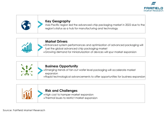
- The market for advanced chip packaging is expected to be dominated by the Asia-Pacific region. One of the main factors promoting market expansion in the Asia Pacific is the region's status as a hub for manufacturing and technology.
- The market for advanced chip packaging is expanding in North America. In terms of AI and ML technologies, North America is at the forefront, focusing on developing state-of-the-art hardware to support these applications. Additionally, the US is adopting more electric vehicles (EVs) and environmentally friendly transportation options.
- Enhanced System Performances, and Optimisation of Advanced Packaging
- Growing Demand for Miniaturisation of Devices
- Exploding Market for Consumer Electronics
- Expensive Pricing Compared to Conventional Semiconductor Packaging
- Thermal Concerns
- Emerging Trends of Fan-out Wafer Level Packaging
- Rapid Technological Advancements
- Growing Semiconductor Industry
- Fan-Out Wafer-Level Packaging (FOWLP) Category Dominant
- Wafer-Level Chip Scale Package (WLCSP) Surges Ahead
- Electronics Expected to be the Leading Segment in the Advanced Chip Packaging Market
- Intel Corporation
- Amkor Technology
- Taiwan Semiconductor Manufacturing Company (TSMC)
- Samsung Electronics
- Advanced Semiconductor Engineering (ASE)
- Siliconware Precision Industries (SPIL)
- JCET Group
- SK Hynix
- Advanced Micro Devices (AMD)
- Powertech Technology Inc. (PTI)
- Flip Chip
- Wafer-Level Packaging
- 5D & 3D Packaging
- Ball Grid Array
- Embedded Die Packaging
- Fan-In Wafer Level Packaging
- Fan-Out Wafer Level Packaging
- Through-Silicon Via (TSV)
- 5D Packaging
- 3D Packaging
- Consumer Electronics
- Automotive
- Healthcare
- Industrial
- Aerospace & Defense
- Organic Substrates
- Bonding Wires
- Lead Frames
- Encapsulation Resins
- Ceramic Packages
- North America
- Europe
- Asia Pacific
- Latin America
- Middle East & Africa
A Look Back and a Look Forward - Comparative Analysis
Some of the major elements driving the growth of the global advanced chip packaging market include the desire for device miniaturisation, improved system performances, and advanced packaging optimisation. In addition, several government initiatives to promote the use of IoT technology to fuel market demand.
The market witnessed staggered growth during the historical period 2018 - 2022. The development of innovative packaging techniques has reduced the cost of installing integrated circuits and improved their output and efficiency; these developments fuelled the market expansion. The demand for advanced chip packaging has also increased because of the increased use of IC in automobiles, which helped the advanced chip packaging market grow.
The complexity of IC design and manufacturing processes is increasing, therefore, foundries need to make investments in cutting-edge machinery to create innovative production systems that keep up with the most recent advancements in the advanced chip packaging industry. Leading foundries like TSMC must make sure that their packaging systems can carry out production utilizing the most recent technologies in addition to continuously upgrading their manufacturing machinery. During the anticipated period, these variables are anticipated to fuel market expansion.
Key Growth Determinants
By providing improved IC containers, the advanced chip packaging business supports the development of next-generation chip designs. The integrated circuit industry has historically employed traditional chip scaling and distinctive architectures for new devices.
Multi-chip packages are also present in every phone, data center, piece of consumer electronics, and network, which encourages system optimisation and furthers the development of advanced chip packaging.
The application of machine learning, AI, and deep learning is encouraged by advanced chip packaging because it makes it possible to connect a range of different processing modules and memories via extremely fast interconnects.
As a result, advanced chip packaging is being used more frequently across several industry verticals, including the automotive, healthcare, aerospace and defense, and industrial sectors. All these traits boost system performance while in use, which serves as a key motivator for market expansion across diverse end-use industries.
As technology develops, manufacturers are concentrating on providing small electronic devices in numerous industry verticals, including healthcare, consumer electronics, automotive, and semiconductor IC manufacturing. To accomplish precise patterning on wafers and chips, these businesses are reducing integrated circuits.
Additionally, due to the sophistication and advancements in wearable and customized healthcare technologies, the market for medical devices is seeing an increase in demand for nano-sized robotic surgery equipment. Small electrical devices are becoming more popular, and thus, designers must use advanced chip packaging instead of more conventional techniques.
The semiconductor industry is experiencing growth in miniaturized electrical devices because of the rising need for high-performance electronics. Due to new semiconductor applications using ultra-thin and ultra-thin dies, which enable the expansion of the global advanced chip packaging sector, miniaturized electronic devices are in great demand.
The market is seeing a lot of new gadgets emerge thanks to recent technological developments, including e-book readers, gaming systems, tablet computers, 3D smart glasses, augmented reality, and virtual reality goods, all of which need high-performance electronic components.
By reducing latency and shortening the critical path, advanced chip packaging technology has helped close the performance gap between processor memory and other types of storage. By shifting the emphasis from device-level scaling to circuit- and system-level scaling, it also enables scaling to proceed effectively.
It is thus anticipated that throughout the projection period, an increase in the shipment of consumer electronics will drive demand for advanced chip packaging.
Major Growth Barriers
Advanced chip packaging methods are more expensive than conventional semiconductor packaging methods. At some points, it becomes too costly to design and manufacture semiconductors for each subsequent node. As more chips and integrated circuits are packaged with intricate designs, the cost of sophisticated packaging increases, limiting their adoption.
Per unit footprint, advanced chip packaging allows extremely dense multi-level integration. Although many applications where miniaturisation is a concern find this appealing, it also poses problems for thermal management because increasing integration raises the on-chip temperature.
Longer design cycles, a greater silicon interposer demand, and a larger form factor are just a few of the problems with advanced chip packaging that need to be fixed.
Key Trends and Opportunities to Look at
Fan-out wafer-level packaging is an advancement above conventional wafer-level packaging in advanced chip packaging. Fan-out wafer-level packaging involves packaging integrated circuits while the wafer is still intact and subsequently chopping it, in contrast to traditional packaging methods where a wafer is first diced.
Fan-out wafer-level packaging features a smaller package footprint and superior thermal and electrical performance compared to conventional packages. Furthermore, while reducing the die size, fan-out wafer-level packaging promotes numerous wafer connections.
The market is being inspired by how quickly technology is developing. Older solutions can easily become outmoded as new packaging methods and materials are created, which can quickly reduce demand and market share for businesses that can't keep up with the most recent developments.
Over the projection period, the semiconductor sector is anticipated to expand rapidly. The foundation of every electronic gadget is made up of semiconductors. Traditional electronic packaging is used after advanced chip packaging for connections. It makes better speed and reliability possible and consumes less power. As a result, the market for advanced chip packaging is growing quickly due to technological developments in semiconductors.
How Does the Regulatory Scenario Shape this Industry?
The devastation caused by the chip scarcity in various industries has highlighted the necessity to build a strong semiconductor ecosystem. To tackle this issue, the 117th United States Congress passed the CHIPS and Science Act, which President Joe Biden signed into law on August 9, 2022.
The act adds over $280 billion in new financing to support American domestic semiconductor manufacture and research. It also includes $39 billion in subsidies for chip manufacture on US territory, along with 25% investment tax credits for prices of manufacturing equipment, including advanced packaging.
Similarly, this decade, the European Union plans to increase its semiconductor self-sufficiency by spending about €43 billion. This is a crucial goal, but getting there means making important trade-offs along multiple roads. The Ministry of Electronics & Information Technology (MeitY) of the Indian government also unveiled four separate programs on December 21 to reduce India's reliance on imports and develop an ecosystem for the semiconductor industry.
Support for all the key stages of semiconductor production, including design, specialty fabs for compound semiconductors, silicon photonics, and sensors, Assembly, Testing, Marking, and Packaging (ATMP) units, display fabs, and semiconductor fabs, is the program's distinguishing feature.
Fairfield’s Ranking Board
Top Segments
The fan-out wafer-level packaging (FOWLP) segment dominated the market in 2022. The rising demand for electronic devices from consumers, technological advancements towards heterogeneous integration, and improved stability and performance of Fan-out wafer level packaging (FOWLP) are all factors contributing to this increase.
Furthermore, modern integrated circuit packages, like FOWLP, have lower costs, higher levels of cost-effective multi-chip module integration, and increased reliability.
Furthermore, the system-in-package (SiP) solutions category is projected to experience the fastest market growth. A variety of factors, including the introduction of 5G network-connected devices, the rising demand for small electronics devices with internet connectivity, and the increase in Internet of Things (IoT) devices, are predicted to propel the growth of the global system in package (SiP) technology sector. In addition, the industry is developing as smartphones and smart wearables are more adopted.
In 2022, the wafer-level chip scale package (WLCSP) category dominated the industry. Due to the rising need for electronic goods that are smaller, lighter, faster, and less expensive, as well as having low-cost packaging and great performance, the wafer-level packaging segment is expanding in the semiconductor packaging sector at the quickest rate.
The semiconductor packaging industry's fast improvements in integrated circuit production are also fostering the expansion of wafer-level packaging technology.
The chip scale package (CSP) category is anticipated to grow substantially throughout the projected period. One of the major factors propelling the growth of the chip-scale package sector is the cheap cost of materials required to manufacture chip-scale packages compared to standard packaging processes.
In 2022, the market was dominated by the electronics sector. Electronics packaging options for semiconductor chips used in wearable technology, computing devices, and consumer electronics are part of the advanced chip packaging market.
To meet the growing need for small, feature-rich electronic devices, the trend involves rising demand for miniaturisation, energy-efficient packaging, and increased connection densities.
The telecommunications category is expected to experience the fastest growth within the forecast time frame. The sector for telecommunications focuses on network infrastructure, high-speed data connectivity, and semiconductor packaging solutions for 5G technologies.
The development of packaging methods to facilitate faster data transmission rates, improved connectivity, and low power consumption in telecommunication systems is a current trend.
Regional Frontrunners
Asia Pacific’s Advanced Chip Packaging Market Largest
The fastest-growing region in the globe is Asia Pacific. Rapid industrialisation and the uptake of cutting-edge technology in the Asia Pacific region are driving an increase in demand for innovative chip packaging solutions.
Asia Pacific has the most lucrative market for advanced chip packaging because of the availability of high-end upgrading technologies, rising demand for smart devices, and expansion in manufacturing industries.
Furthermore, several helpful non-profit organisations are major contributors to the advancement of packaging technology. These businesses take a variety of steps to build better power infrastructure, which stimulates the growth of the advanced chip packaging sector in the area.
The region's emphasis on IoT applications, 5G deployment, and smart manufacturing drives demand for cutting-edge advanced chip packaging methods.
Smart Machinery Presents Gains to North America
The North American area accounts for the second-largest portion of the global market for advanced chip packaging. The rise in North American consumers' disposable income is what fuels sales of advanced chip packaging.
The adoption of creative packaging solutions has increased because of the need from various industries for clever and smart machinery and technology platforms.
The energy and power sector is using more advanced technologies, which is accelerating market expansion. Additionally, it is anticipated that the incorporation of microprocessors and microcontrollers in consumer electronics and electric cars will boost the market for advanced chip packaging during the forecast period.
The growing demand for EVs and environmentally friendly transportation options will be the driving force behind the US market for advanced chip packaging solutions with high dependability, effective thermal management, and tiny form factors.
Fairfield’s Competitive Landscape Analysis
The advanced chip packaging market is a congested industry with few significant players operating worldwide. To increase their global footprint, the major firms are launching new items and enhancing their distribution networks. In addition, Fairfield Market Research anticipates that during the next few years, there will be further market consolidation.
Who are the Leaders in Global Advanced Chip Packaging Space?
Global Advanced Chip Packaging Market is Segmented as Below:
By Packaging Type
By Technology
By End User
By Material
By Region
- Executive Summary
- Global Advanced Chip Packaging Market Snapshot
- Future Projections
- Key Market Trends
- Regional Snapshot, by Value, 2026
- Analyst Recommendations
- Market Overview
- Market Definitions and Segmentations
- Market Dynamics
- Drivers
- Restraints
- Market Opportunities
- Value Chain Analysis
- COVID-19 Impact Analysis
- Porter's Five Forces Analysis
- Impact of Russia-Ukraine Conflict
- PESTLE Analysis
- Regulatory Analysis
- Price Trend Analysis
- Current Prices and Future Projections, 2025-2033
- Price Impact Factors
- Global Advanced Chip Packaging Market Outlook, 2020 - 2033
- Global Advanced Chip Packaging Market Outlook, by Packaging Type, Value (US$ Bn), 2020-2033
- Flip Chip
- Wafer-Level Packaging
- 5D & 3D Packaging
- Ball Grid Array
- Embedded Die Packaging
- Global Advanced Chip Packaging Market Outlook, by Technology, Value (US$ Bn), 2020-2033
- Fan-In Wafer Level Packaging
- Fan-Out Wafer Level Packaging
- Through-Silicon Via (TSV)
- 5D Packaging
- 3D Packaging
- Global Advanced Chip Packaging Market Outlook, by End User, Value (US$ Bn), 2020-2033
- Consumer Electronics
- Automotive
- Healthcare
- Industrial
- Aerospace & Defense
- Global Advanced Chip Packaging Market Outlook, by Material, Value (US$ Bn), 2020-2033
- Organic Substrates
- Bonding Wires
- Lead Frames
- Encapsulation Resins
- Ceramic Packages
- Global Advanced Chip Packaging Market Outlook, by Region, Value (US$ Bn), 2020-2033
- North America
- Europe
- Asia Pacific
- Latin America
- Middle East & Africa
- Global Advanced Chip Packaging Market Outlook, by Packaging Type, Value (US$ Bn), 2020-2033
- North America Advanced Chip Packaging Market Outlook, 2020 - 2033
- North America Advanced Chip Packaging Market Outlook, by Packaging Type, Value (US$ Bn), 2020-2033
- Flip Chip
- Wafer-Level Packaging
- 5D & 3D Packaging
- Ball Grid Array
- Embedded Die Packaging
- North America Advanced Chip Packaging Market Outlook, by Technology, Value (US$ Bn), 2020-2033
- Fan-In Wafer Level Packaging
- Fan-Out Wafer Level Packaging
- Through-Silicon Via (TSV)
- 5D Packaging
- 3D Packaging
- North America Advanced Chip Packaging Market Outlook, by End User, Value (US$ Bn), 2020-2033
- Consumer Electronics
- Automotive
- Healthcare
- Industrial
- Aerospace & Defense
- North America Advanced Chip Packaging Market Outlook, by Material, Value (US$ Bn), 2020-2033
- Organic Substrates
- Bonding Wires
- Lead Frames
- Encapsulation Resins
- Ceramic Packages
- North America Advanced Chip Packaging Market Outlook, by Country, Value (US$ Bn), 2020-2033
- U.S. Advanced Chip Packaging Market Outlook, by Packaging Type, 2020-2033
- U.S. Advanced Chip Packaging Market Outlook, by Technology, 2020-2033
- U.S. Advanced Chip Packaging Market Outlook, by End User, 2020-2033
- U.S. Advanced Chip Packaging Market Outlook, by Material, 2020-2033
- Canada Advanced Chip Packaging Market Outlook, by Packaging Type, 2020-2033
- Canada Advanced Chip Packaging Market Outlook, by Technology, 2020-2033
- Canada Advanced Chip Packaging Market Outlook, by End User, 2020-2033
- Canada Advanced Chip Packaging Market Outlook, by Material, 2020-2033
- BPS Analysis/Market Attractiveness Analysis
- North America Advanced Chip Packaging Market Outlook, by Packaging Type, Value (US$ Bn), 2020-2033
- Europe Advanced Chip Packaging Market Outlook, 2020 - 2033
- Europe Advanced Chip Packaging Market Outlook, by Packaging Type, Value (US$ Bn), 2020-2033
- Flip Chip
- Wafer-Level Packaging
- 5D & 3D Packaging
- Ball Grid Array
- Embedded Die Packaging
- Europe Advanced Chip Packaging Market Outlook, by Technology, Value (US$ Bn), 2020-2033
- Fan-In Wafer Level Packaging
- Fan-Out Wafer Level Packaging
- Through-Silicon Via (TSV)
- 5D Packaging
- 3D Packaging
- Europe Advanced Chip Packaging Market Outlook, by End User, Value (US$ Bn), 2020-2033
- Consumer Electronics
- Automotive
- Healthcare
- Industrial
- Aerospace & Defense
- Europe Advanced Chip Packaging Market Outlook, by Material, Value (US$ Bn), 2020-2033
- Organic Substrates
- Bonding Wires
- Lead Frames
- Encapsulation Resins
- Ceramic Packages
- Europe Advanced Chip Packaging Market Outlook, by Country, Value (US$ Bn), 2020-2033
- Germany Advanced Chip Packaging Market Outlook, by Packaging Type, 2020-2033
- Germany Advanced Chip Packaging Market Outlook, by Technology, 2020-2033
- Germany Advanced Chip Packaging Market Outlook, by End User, 2020-2033
- Germany Advanced Chip Packaging Market Outlook, by Material, 2020-2033
- Italy Advanced Chip Packaging Market Outlook, by Packaging Type, 2020-2033
- Italy Advanced Chip Packaging Market Outlook, by Technology, 2020-2033
- Italy Advanced Chip Packaging Market Outlook, by End User, 2020-2033
- Italy Advanced Chip Packaging Market Outlook, by Material, 2020-2033
- France Advanced Chip Packaging Market Outlook, by Packaging Type, 2020-2033
- France Advanced Chip Packaging Market Outlook, by Technology, 2020-2033
- France Advanced Chip Packaging Market Outlook, by End User, 2020-2033
- France Advanced Chip Packaging Market Outlook, by Material, 2020-2033
- U.K. Advanced Chip Packaging Market Outlook, by Packaging Type, 2020-2033
- U.K. Advanced Chip Packaging Market Outlook, by Technology, 2020-2033
- U.K. Advanced Chip Packaging Market Outlook, by End User, 2020-2033
- U.K. Advanced Chip Packaging Market Outlook, by Material, 2020-2033
- Spain Advanced Chip Packaging Market Outlook, by Packaging Type, 2020-2033
- Spain Advanced Chip Packaging Market Outlook, by Technology, 2020-2033
- Spain Advanced Chip Packaging Market Outlook, by End User, 2020-2033
- Spain Advanced Chip Packaging Market Outlook, by Material, 2020-2033
- Russia Advanced Chip Packaging Market Outlook, by Packaging Type, 2020-2033
- Russia Advanced Chip Packaging Market Outlook, by Technology, 2020-2033
- Russia Advanced Chip Packaging Market Outlook, by End User, 2020-2033
- Russia Advanced Chip Packaging Market Outlook, by Material, 2020-2033
- Rest of Europe Advanced Chip Packaging Market Outlook, by Packaging Type, 2020-2033
- Rest of Europe Advanced Chip Packaging Market Outlook, by Technology, 2020-2033
- Rest of Europe Advanced Chip Packaging Market Outlook, by End User, 2020-2033
- Rest of Europe Advanced Chip Packaging Market Outlook, by Material, 2020-2033
- BPS Analysis/Market Attractiveness Analysis
- Europe Advanced Chip Packaging Market Outlook, by Packaging Type, Value (US$ Bn), 2020-2033
- Asia Pacific Advanced Chip Packaging Market Outlook, 2020 - 2033
- Asia Pacific Advanced Chip Packaging Market Outlook, by Packaging Type, Value (US$ Bn), 2020-2033
- Flip Chip
- Wafer-Level Packaging
- 5D & 3D Packaging
- Ball Grid Array
- Embedded Die Packaging
- Asia Pacific Advanced Chip Packaging Market Outlook, by Technology, Value (US$ Bn), 2020-2033
- Fan-In Wafer Level Packaging
- Fan-Out Wafer Level Packaging
- Through-Silicon Via (TSV)
- 5D Packaging
- 3D Packaging
- Asia Pacific Advanced Chip Packaging Market Outlook, by End User, Value (US$ Bn), 2020-2033
- Consumer Electronics
- Automotive
- Healthcare
- Industrial
- Aerospace & Defense
- Asia Pacific Advanced Chip Packaging Market Outlook, by Material, Value (US$ Bn), 2020-2033
- Organic Substrates
- Bonding Wires
- Lead Frames
- Encapsulation Resins
- Ceramic Packages
- Asia Pacific Advanced Chip Packaging Market Outlook, by Country, Value (US$ Bn), 2020-2033
- China Advanced Chip Packaging Market Outlook, by Packaging Type, 2020-2033
- China Advanced Chip Packaging Market Outlook, by Technology, 2020-2033
- China Advanced Chip Packaging Market Outlook, by End User, 2020-2033
- China Advanced Chip Packaging Market Outlook, by Material, 2020-2033
- Japan Advanced Chip Packaging Market Outlook, by Packaging Type, 2020-2033
- Japan Advanced Chip Packaging Market Outlook, by Technology, 2020-2033
- Japan Advanced Chip Packaging Market Outlook, by End User, 2020-2033
- Japan Advanced Chip Packaging Market Outlook, by Material, 2020-2033
- South Korea Advanced Chip Packaging Market Outlook, by Packaging Type, 2020-2033
- South Korea Advanced Chip Packaging Market Outlook, by Technology, 2020-2033
- South Korea Advanced Chip Packaging Market Outlook, by End User, 2020-2033
- South Korea Advanced Chip Packaging Market Outlook, by Material, 2020-2033
- India Advanced Chip Packaging Market Outlook, by Packaging Type, 2020-2033
- India Advanced Chip Packaging Market Outlook, by Technology, 2020-2033
- India Advanced Chip Packaging Market Outlook, by End User, 2020-2033
- India Advanced Chip Packaging Market Outlook, by Material, 2020-2033
- Southeast Asia Advanced Chip Packaging Market Outlook, by Packaging Type, 2020-2033
- Southeast Asia Advanced Chip Packaging Market Outlook, by Technology, 2020-2033
- Southeast Asia Advanced Chip Packaging Market Outlook, by End User, 2020-2033
- Southeast Asia Advanced Chip Packaging Market Outlook, by Material, 2020-2033
- Rest of SAO Advanced Chip Packaging Market Outlook, by Packaging Type, 2020-2033
- Rest of SAO Advanced Chip Packaging Market Outlook, by Technology, 2020-2033
- Rest of SAO Advanced Chip Packaging Market Outlook, by End User, 2020-2033
- Rest of SAO Advanced Chip Packaging Market Outlook, by Material, 2020-2033
- BPS Analysis/Market Attractiveness Analysis
- Asia Pacific Advanced Chip Packaging Market Outlook, by Packaging Type, Value (US$ Bn), 2020-2033
- Latin America Advanced Chip Packaging Market Outlook, 2020 - 2033
- Latin America Advanced Chip Packaging Market Outlook, by Packaging Type, Value (US$ Bn), 2020-2033
- Flip Chip
- Wafer-Level Packaging
- 5D & 3D Packaging
- Ball Grid Array
- Embedded Die Packaging
- Latin America Advanced Chip Packaging Market Outlook, by Technology, Value (US$ Bn), 2020-2033
- Fan-In Wafer Level Packaging
- Fan-Out Wafer Level Packaging
- Through-Silicon Via (TSV)
- 5D Packaging
- 3D Packaging
- Latin America Advanced Chip Packaging Market Outlook, by End User, Value (US$ Bn), 2020-2033
- Consumer Electronics
- Automotive
- Healthcare
- Industrial
- Aerospace & Defense
- Latin America Advanced Chip Packaging Market Outlook, by Material, Value (US$ Bn), 2020-2033
- Organic Substrates
- Bonding Wires
- Lead Frames
- Encapsulation Resins
- Ceramic Packages
- Latin America Advanced Chip Packaging Market Outlook, by Country, Value (US$ Bn), 2020-2033
- Brazil Advanced Chip Packaging Market Outlook, by Packaging Type, 2020-2033
- Brazil Advanced Chip Packaging Market Outlook, by Technology, 2020-2033
- Brazil Advanced Chip Packaging Market Outlook, by End User, 2020-2033
- Brazil Advanced Chip Packaging Market Outlook, by Material, 2020-2033
- Mexico Advanced Chip Packaging Market Outlook, by Packaging Type, 2020-2033
- Mexico Advanced Chip Packaging Market Outlook, by Technology, 2020-2033
- Mexico Advanced Chip Packaging Market Outlook, by End User, 2020-2033
- Mexico Advanced Chip Packaging Market Outlook, by Material, 2020-2033
- Argentina Advanced Chip Packaging Market Outlook, by Packaging Type, 2020-2033
- Argentina Advanced Chip Packaging Market Outlook, by Technology, 2020-2033
- Argentina Advanced Chip Packaging Market Outlook, by End User, 2020-2033
- Argentina Advanced Chip Packaging Market Outlook, by Material, 2020-2033
- Rest of LATAM Advanced Chip Packaging Market Outlook, by Packaging Type, 2020-2033
- Rest of LATAM Advanced Chip Packaging Market Outlook, by Technology, 2020-2033
- Rest of LATAM Advanced Chip Packaging Market Outlook, by End User, 2020-2033
- Rest of LATAM Advanced Chip Packaging Market Outlook, by Material, 2020-2033
- BPS Analysis/Market Attractiveness Analysis
- Latin America Advanced Chip Packaging Market Outlook, by Packaging Type, Value (US$ Bn), 2020-2033
- Middle East & Africa Advanced Chip Packaging Market Outlook, 2020 - 2033
- Middle East & Africa Advanced Chip Packaging Market Outlook, by Packaging Type, Value (US$ Bn), 2020-2033
- Flip Chip
- Wafer-Level Packaging
- 5D & 3D Packaging
- Ball Grid Array
- Embedded Die Packaging
- Middle East & Africa Advanced Chip Packaging Market Outlook, by Technology, Value (US$ Bn), 2020-2033
- Fan-In Wafer Level Packaging
- Fan-Out Wafer Level Packaging
- Through-Silicon Via (TSV)
- 5D Packaging
- 3D Packaging
- Middle East & Africa Advanced Chip Packaging Market Outlook, by End User, Value (US$ Bn), 2020-2033
- Consumer Electronics
- Automotive
- Healthcare
- Industrial
- Aerospace & Defense
- Middle East & Africa Advanced Chip Packaging Market Outlook, by Material, Value (US$ Bn), 2020-2033
- Organic Substrates
- Bonding Wires
- Lead Frames
- Encapsulation Resins
- Ceramic Packages
- Middle East & Africa Advanced Chip Packaging Market Outlook, by Country, Value (US$ Bn), 2020-2033
- GCC Advanced Chip Packaging Market Outlook, by Packaging Type, 2020-2033
- GCC Advanced Chip Packaging Market Outlook, by Technology, 2020-2033
- GCC Advanced Chip Packaging Market Outlook, by End User, 2020-2033
- GCC Advanced Chip Packaging Market Outlook, by Material, 2020-2033
- South Africa Advanced Chip Packaging Market Outlook, by Packaging Type, 2020-2033
- South Africa Advanced Chip Packaging Market Outlook, by Technology, 2020-2033
- South Africa Advanced Chip Packaging Market Outlook, by End User, 2020-2033
- South Africa Advanced Chip Packaging Market Outlook, by Material, 2020-2033
- Egypt Advanced Chip Packaging Market Outlook, by Packaging Type, 2020-2033
- Egypt Advanced Chip Packaging Market Outlook, by Technology, 2020-2033
- Egypt Advanced Chip Packaging Market Outlook, by End User, 2020-2033
- Egypt Advanced Chip Packaging Market Outlook, by Material, 2020-2033
- Nigeria Advanced Chip Packaging Market Outlook, by Packaging Type, 2020-2033
- Nigeria Advanced Chip Packaging Market Outlook, by Technology, 2020-2033
- Nigeria Advanced Chip Packaging Market Outlook, by End User, 2020-2033
- Nigeria Advanced Chip Packaging Market Outlook, by Material, 2020-2033
- Rest of Middle East Advanced Chip Packaging Market Outlook, by Packaging Type, 2020-2033
- Rest of Middle East Advanced Chip Packaging Market Outlook, by Technology, 2020-2033
- Rest of Middle East Advanced Chip Packaging Market Outlook, by End User, 2020-2033
- Rest of Middle East Advanced Chip Packaging Market Outlook, by Material, 2020-2033
- BPS Analysis/Market Attractiveness Analysis
- Middle East & Africa Advanced Chip Packaging Market Outlook, by Packaging Type, Value (US$ Bn), 2020-2033
- Competitive Landscape
- Company Vs Segment Heatmap
- Company Market Share Analysis, 2025
- Competitive Dashboard
- Company Profiles
- Intel Corporation
- Company Overview
- Product Portfolio
- Financial Overview
- Business Strategies and Developments
- Amkor Technology
- Taiwan Semiconductor Manufacturing Company (TSMC)
- Samsung Electronics
- Advanced Semiconductor Engineering (ASE)
- Siliconware Precision Industries (SPIL)
- JCET Group
- SK Hynix
- Advanced Micro Devices (AMD)
- Powertech Technology Inc. (PTI)
- Intel Corporation
- Appendix
- Research Methodology
- Report Assumptions
- Acronyms and Abbreviations
|
zBASE YEAR |
HISTORICAL DATA |
FORECAST PERIOD |
UNITS |
|||
 |
2020 |
 |
2020 - 2025 |
 |
2026 - 2033 |
Value: US$ Billion |
|
REPORT FEATURES |
DETAILS |
|
Technology Coverage |
|
|
Application Coverage |
|
|
End-use Industry Coverage |
|
|
Geographical Coverage |
|
|
Leading Companies |
|
|
Report Highlights |
Key Market Indicators, Macro-micro economic impact analysis, Technological Roadmap, Key Trends, Driver, Restraints, and Future Opportunities & Revenue Pockets, Porter’s 5 Forces Analysis, Historical Trend (2019-2021), Market Estimates and Forecast, Market Dynamics, Industry Trends, Competition Landscape, Category, Region, Country wise Trends & Analysis, COVID-19 Impact Analysis (Demand and Supply Chain) |
Our Research Methodology
Considering the volatility of business today, traditional approaches to strategizing a game plan can be unfruitful if not detrimental. True ambiguity is no way to determine a forecast. A myriad of predetermined factors must be accounted for such as the degree of risk involved, the magnitude of circumstances, as well as conditions or consequences that are not known or unpredictable. To circumvent binary views that cast uncertainty, the application of market research intelligence to strategically posture, move, and enable actionable outcomes is necessary.
View Methodology
Quality Assured
Rigorous Validation Process

Confidentiality Assured
End-to-end Data Security

Custom Research Services
Tailored To Your Objectives
FAQs
The Advanced Chip Packaging market is expected to reach USD 47.5 Billion in 2026.
The Advanced Chip Packaging market is projected to expand at a 6.9% CAGR through 2033.
The market is driven by growing demand for device miniaturization, enhanced system performance, and rising adoption of consumer electronics.
Asia Pacific is the dominant regional market for Advanced Chip Packaging.
Intel Corporation, Taiwan Semiconductor Manufacturing Company (TSMC), Samsung Electronics, Amkor Technology, and Advanced Semiconductor Engineering (ASE) are some leading industry players in the Advanced Chip Packaging marke
Related Reports
Helicopter Meteorological Software Market Size, Share, Insights, Competitive Landscape, and Forecast 2026 to 2033
The global helicopter meteorological software market is valued at US$130.64 million in 2026, reaching US$181.40 million by 2033, growing at a 4.80% CAGR
Teleoperations Market Size, Share, Insights, Competitive Landscape, and Forecast 2026 to 2033
The global teleoperations market is valued at US$650.00 million in 2026, reaching US$2,540.70 million by 2033, growing at a 21.50% CAGR
Pedestrian Entrance Control Systems Market Size, Share, Insights, Competitive Landscape, and Forecast 2026 to 2033
The global pedestrian entrance control systems market is valued at US$2.00 billion in 2026, reaching US$3.40 billion by 2033, growing at a 7.88% CAGR
Modular UPS Market Size, Share, Insights, Competitive Landscape, and Forecast 2026 to 2033
The global modular UPS market is valued at US$3.06209 billion in 2026, reaching US$5.03731 billion by 2033, growing at a 7.37% CAGR
Facility Management Market Size, Share, Insights, Competitive Landscape, and Forecast 2026 to 2033
The global facility management market is valued at US$1,560.35 billion in 2026, reaching US$2,894.52 billion by 2033, growing at a 9.23% CAGR
Agriculture Drone Market Size, Share, Insights, Competitive Landscape, and Forecast 2026 to 2033
The global agriculture drone market is valued at US$3.90 billion in 2026, reaching US$13.20 billion by 2033, growing at a 19.03% CAGR