



2D Material Transistor Market
2D Material Transistor Market Size, Share, Insights, Competitive Landscape, and Forecast 2026 to 2033
2D Material Transistor Market Size and Trend Analysis
What Is the Growth Outlook for 2D Material Transistors?
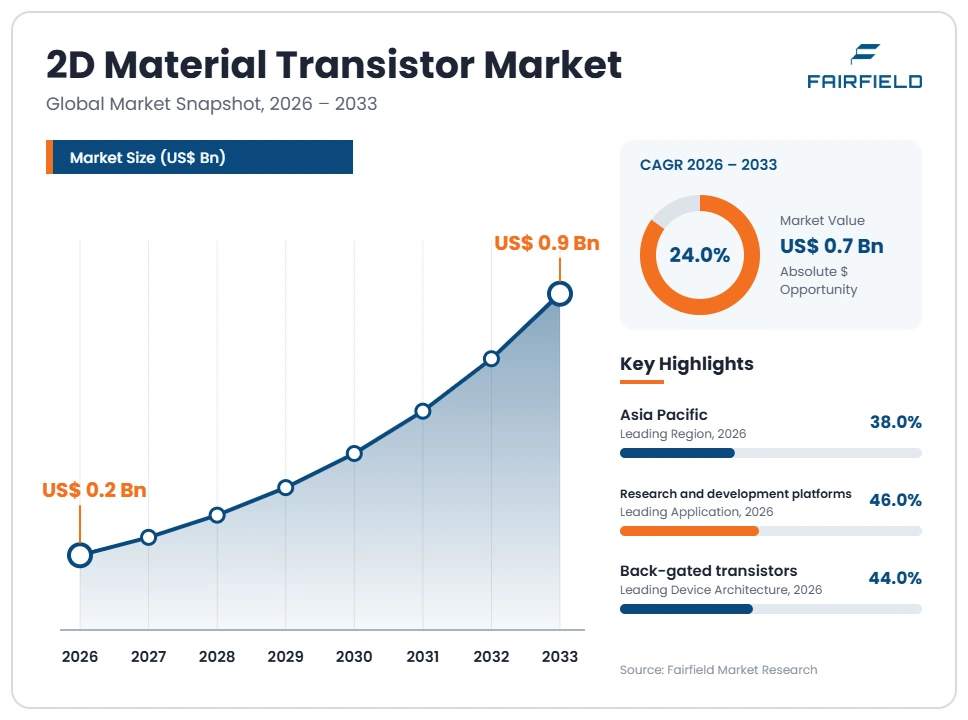
The global 2D material transistor market size is expected to be valued at US$ 0.2 billion in 2026 and projected to reach US$ 0.9 billion by 2033, growing at a CAGR of 24.0% between 2026 and 2033.
Precisely, revenue stands at about US$ 205 million in 2026 and reaches roughly US$ 922 million by 2033, after expanding at a 21.6% CAGR from around US$ 62 million in 2020. This is a research and early-prototype field, not a production industry. Spending flows into materials and substrates, characterisation equipment, prototype fabrication and a small number of sensor products. Three factors set the pace: sustained public semiconductor research funding, the search for channel materials beyond silicon at future nodes, and growing university and institute capacity for device fabrication. Growth is therefore a research-to-pilot ramp off a very small base, and a high percentage rate reflects that base rather than commercial manufacturing volume.
Key Report Takeaways
- By Material Type: Graphene held 41% share in 2026, while molybdenum disulphide is projected to expand at a 27.2% CAGR through 2033, driven by its semiconducting band gap and suitability for switching channels.
- By Device Architecture: Back-gated transistors held 44% share in 2026, while dual-gate and gate-all-around prototypes are projected to expand at a 29.1% CAGR through 2033, driven by stacked channel experiments on test wafers.
- By Offering: Materials and substrates held 37% share in 2026, while prototype fabrication and foundry services are projected to expand at a 28.4% CAGR through 2033, driven by shared multi-project wafer access for academic groups.
- By Application: Research and development platforms held 46% share in 2026, while logic and memory device prototypes are projected to expand at a 29.6% CAGR through 2033, driven by roadmap evaluation of beyond-silicon channel options.
- By Geography: Asia Pacific held 38% share in 2026, while North America is projected to expand at a 26.8% CAGR through 2033, driven by federal research funding and university-to-foundry prototyping access.
Global 2D Material Transistor Market Trends and Insights
Drivers Impact Analysis
Two forces account for most research spending on atomically thin channel devices through the forecast period.
| Driver | Impact on CAGR Forecast | Geographic Relevance | Impact Timeline |
| Roadmap search for channel materials beyond silicon | High | Global | Long term ≥4 years |
| Public semiconductor research funding programmes | High | North America, Europe, Asia Pacific | Medium term 2–4 years |
Silicon Channel Scaling Limits Put Two-Dimensional Semiconductors on the Device Roadmap
Device scaling pressure is the primary reason research budgets reach atomically thin channels at all. As silicon fins and nanosheets thin toward a few nanometres, surface roughness scattering and leakage degrade electrostatic control. A monolayer semiconductor is uniformly thin by construction, which preserves gate control at very short channel lengths. That physical argument keeps two-dimensional channels inside long-range device planning and sustains steady, non-cyclical experimental demand.
The mechanism is roadmap-driven rather than customer-driven. The International Roadmap for Devices and Systems lists two-dimensional channel materials among candidate options for nodes beyond conventional silicon scaling. Roadmap inclusion justifies exploratory programmes inside advanced logic research groups, and it directs university work toward transition metal dichalcogenides such as molybdenum disulphide and tungsten diselenide. Each programme purchases substrates, growth reactors, probe stations and electron microscopy time, which is where current revenue sits.
Public Semiconductor Funding Programmes Underwrite Pilot Lines for Atomically Thin Devices
Government funding, not commercial procurement, pays for most two-dimensional transistor work today. Large national and regional semiconductor programmes finance research centres, shared cleanrooms and pilot equipment that academic groups could never buy alone. Because this money is appropriated over multi-year horizons, it gives suppliers of growth reactors, metrology tools and specialist wafers unusually visible demand for a pre-commercial field.
The causal chain runs from policy to equipment orders. The CHIPS and Science Act in the United States and the European Chips Act both fund advanced semiconductor research infrastructure, including exploratory device work. Institutes use those grants to install chemical vapour deposition systems, atomic layer deposition tools for hexagonal boron nitride dielectrics, and atomic force and Raman characterisation platforms. Shared pilot lines then offer fabrication slots to smaller groups, multiplying the number of teams able to build atomically thin devices.
Restraints Impact Analysis
Two technical constraints prevent two-dimensional channel devices from moving into manufacturing.
| Restraint | Impact on CAGR Forecast | Geographic Relevance | Impact Timeline |
| Wafer-scale growth uniformity and contact resistance | High | Global | Long term ≥4 years |
| Absence of metrology and qualification standards | Medium | Global | Long term ≥4 years |
Wafer-Scale Growth Uniformity and Contact Resistance Block Manufacturable Device Flows
No qualified process flow exists for atomically thin channel transistors, which is why this field has no volume manufacturing. Laboratory devices perform well individually, but performance collapses when thousands must behave identically across a wafer. Grain boundaries, sulphur vacancies, wrinkles and transfer residues vary from die to die. Without uniformity, there is no yield, and without yield there is no production order to size.
Two technical causes dominate. Chemical vapour deposition of monolayer films produces polycrystalline material whose domain size and defect density vary with temperature and precursor flow across a three hundred millimetre wafer. Separately, metal contacts to a monolayer form Fermi-level pinning and Schottky barriers, so contact resistance consumes much of the drive current advantage. Semi-metal and transferred contact schemes improve results in the laboratory but add process steps that are difficult to repeat.
Missing Metrology and Qualification Standards Keep Purchases Inside Research Budgets
Procurement stays in research budgets because no qualification framework exists for atomically thin devices. Industrial buyers require reliability data, accelerated life testing protocols and accepted inspection methods before committing to a technology. For two-dimensional channels, there is no mature standard defining acceptable defect density, layer count verification or interface trap measurement. Without those definitions, purchasing cannot be justified as a production investment.
The cause is the immaturity of measurement itself. Established semiconductor metrology assumes bulk films thick enough for optical and electrical inspection; a single atomic layer defeats many of those techniques. Raman spectroscopy and photoluminescence mapping indicate layer number and strain but are slow and not fully standardised for inline use. Bias temperature instability and dielectric breakdown behaviour in stacked two-dimensional systems remain under study, so reliability models that fabs depend upon simply do not yet exist.
Market Opportunities
Atomically Thin Gas and Biosensors Open the First Commercial Revenue Pool
Sensing is the one application where atomically thin devices can generate product revenue before a qualified logic process exists. A monolayer channel is entirely surface, so adsorbed molecules shift conductance strongly. That gives detection limits unreachable with bulk silicon sensors. Crucially, a sensor sells on sensitivity and selectivity rather than on billions of identical transistors, so modest device yield is commercially tolerable.
Specialist instrument makers and diagnostics developers are positioned to capture this pool, working with graphene and transition metal dichalcogenide suppliers. Demand comes from environmental monitoring of nitrogen dioxide and volatile organic compounds, industrial leak detection, and point-of-care biomarker testing where sample volumes are tiny. Progress in wafer-scale graphene growth and in passivation using hexagonal boron nitride improves device stability and drift, which has been the main obstacle to commercial sensor qualification.
Wafer Supply and Multi-Project Prototyping Services Create Recurring Revenue From Research Budgets
Selling access rather than devices is the most dependable revenue pool in this field. Research groups need monolayer films on specific substrates, clean transfer, lithography and electrical characterisation, yet few can justify a dedicated cleanroom. Shared prototyping services convert that need into repeatable orders, and the same customers return each funding cycle, which gives suppliers more predictable income than one-off equipment sales.
Materials houses, university cleanrooms and institute pilot lines are best placed to capture it. Demand comes from physics and electrical engineering departments, national laboratories and corporate exploratory research teams evaluating beyond-silicon options. Multi-project wafer runs let several groups share mask and processing costs, lowering the entry price for a prototype. Expanding public research infrastructure, funded through national semiconductor programmes, directly increases the number of groups able to commission this work.
Segment Analysis
- By Material Type: Graphene Leads Supply While Molybdenum Disulphide Gains Research Momentum
Graphene held 41% share in 2026, the largest material position, because its supply chain is the most developed and its applications extend beyond transistors into sensors, electrodes and composites. Molybdenum disulphide is the fastest-growing material at a 27.2% CAGR through 2033, for a simple physical reason: graphene has no band gap, so it cannot switch off cleanly, while a monolayer of molybdenum disulphide offers a direct band gap suitable for logic channels. Other transition metal dichalcogenides, including tungsten disulphide and tungsten diselenide, expand as complementary n-type and p-type options. Hexagonal boron nitride grows as the preferred dielectric and encapsulation layer. The implication for suppliers is that revenue mix is shifting from carbon materials toward semiconducting chalcogenides and the dielectrics needed to build a complete device stack.
- By Device Architecture: Back-Gated Structures Dominate Laboratories While Gate-All-Around Prototypes Accelerate
Back-gated transistors accounted for 44% of activity in 2026 because they are the fastest structure to build. A flake or film placed on an oxidised silicon wafer gives a working device with minimal processing, which suits material screening and mobility measurement. Dual-gate and gate-all-around prototypes are the fastest-growing architecture at a 29.1% CAGR to 2033, since these structures test whether atomically thin channels can meet the electrostatic requirements of advanced nodes. Top-gated devices sit between the two and depend on high-quality dielectric deposition onto an inert surface. Flexible thin-film transistors form a separate branch aimed at bendable displays and wearable sensors. The practical consequence is rising demand for atomic layer deposition, transfer tooling and precise alignment capability rather than for simple exfoliation workflows.
- By Offering: Materials and Substrates Hold the Largest Share While Prototyping Services Expand Quickest
Materials and substrates represented 37% of spending in 2026, as nearly every project begins by buying films, crystals or coated wafers. Prototype fabrication and foundry services are the fastest-growing offering at a 28.4% CAGR to 2033, because shared facilities let small teams build devices without owning a cleanroom. Characterisation and metrology equipment, including Raman systems, atomic force microscopes and probe stations, remains a substantial and steady category. Licensing and intellectual property is small today but matters strategically, since patent positions on growth, transfer and contact engineering will shape any future commercial phase. The business implication is that suppliers who bundle material, processing and measurement into a service relationship capture far more value per customer than those selling consumables alone.
- By Application: Research Platforms Lead Spending While Logic and Memory Prototypes Grow Fastest
Research and development platforms absorbed 46% of spending in 2026, which confirms the pre-commercial character of this field. Universities, institutes and corporate laboratories buy materials and tool time to investigate device physics rather than to ship products. Logic and memory device prototypes are the fastest-growing application at a 29.6% CAGR to 2033, reflecting roadmap evaluation of beyond-silicon channel options and interest in two-dimensional selectors for dense memory arrays. Sensors and biosensors form the nearest-term commercial outlet. Radio-frequency devices exploit high carrier velocity for high-frequency circuits, while flexible and printed electronics target conformable displays and skin-mounted monitoring. The strategic implication is clear: revenue today follows research intent, and any shift toward product applications will arrive first through sensing, not computing.
Geography Analysis
- Which Region Is Growing Fastest in the 2D Material Transistor Market?
North America is growing fastest in the 2D material transistor market at a 26.8% CAGR between 2026 and 2033, from 28% share in 2026. The United States supplies almost all of this activity, with Canada contributing through university nanofabrication centres. Growth is driven by federal semiconductor research funding under the CHIPS and Science Act, which supports shared cleanrooms, pilot equipment and exploratory device programmes. National laboratories and leading research universities operate the instrumentation base, and corporate exploratory groups fund targeted work on contacts and dielectric integration. Venture capital backs a thin layer of materials and sensor start-ups. The main constraint is the distance between laboratory results and a qualified process, so funding renewals depend on demonstrated progress in uniformity and reliability rather than on single-device performance records.
- Europe Builds Atomically Thin Device Capability Through Coordinated Public Research Infrastructure
Europe held 26% share in 2026 and grows at a 23.1% CAGR, with capability concentrated in Germany, the United Kingdom, Spain, Sweden, Italy and the Netherlands. The region’s strength is coordination: the Graphene Flagship built a durable network linking universities, institutes and materials suppliers, and the European Chips Act now channels funding toward advanced semiconductor research infrastructure and pilot lines. Shared institute facilities give smaller groups access to deposition, lithography and electron microscopy. Materials companies supplying monolayer films and crystals are unusually well represented relative to the region’s share of chip manufacturing. The persistent barrier is translation, as strong publication output has not converted into device commercialisation. The clearest opportunity lies in sensing and flexible electronics, where European instrument and medical device firms can absorb early prototypes.
- Which Region Is Leading the 2D Material Transistor Market?
Asia Pacific leads the 2D material transistor market with 38% share in 2026, reflecting the scale of its research output and its proximity to advanced semiconductor manufacturing. China produces the largest volume of published device work and hosts extensive graphene and chalcogenide material supply. Japan contributes high-quality hexagonal boron nitride crystal growth and long-standing materials science depth. South Korea and Taiwan connect exploratory device research directly to advanced logic development, while India and Singapore expand university nanofabrication capacity. Regional growth of 24.2% reflects heavy state research spending and a large graduate pipeline. The structural advantage is adjacency: researchers can access process expertise, metrology and wafer handling practice from established fabs, which shortens the path from a laboratory recipe to a repeatable wafer-scale process.
- Latin America Participates Through University Groups and Materials Characterisation Research
Latin America accounts for 4% share in 2026 and grows at a 19.5% CAGR, the slowest regional rate, with activity concentrated in Brazil and Mexico. Work centres on materials synthesis, Raman characterisation and sensor demonstrations rather than on transistor fabrication, because few institutions operate the cleanroom infrastructure required for gated device flows. University groups collaborate internationally and often send samples abroad for device processing. Barriers are financial and structural: research budgets are constrained, imported substrates and precursors carry duty and long lead times, and there is no regional semiconductor pilot line. The realistic opportunity is in sensing applications tied to agriculture, mining and environmental monitoring, where locally relevant problems justify funding and where a sensor can reach usefulness without a qualified transistor process.
- Middle East & Africa Advances Through Sovereign Research Universities and Materials Programmes
Middle East & Africa holds 4% share in 2026 and expands at a 20.4% CAGR, with capability clustered in Saudi Arabia, the United Arab Emirates, Israel and South Africa. Sovereign-funded research universities have invested in nanofabrication and characterisation facilities, and national diversification strategies treat advanced materials as a priority. Israel contributes device physics depth and start-up formation. Barriers include a small domestic electronics manufacturing base, limited specialist supply chains and dependence on imported precursors and tools. Researcher retention is an additional constraint. The most promising opportunity is desalination, energy and environmental sensing, where atomically thin sensors address regional priorities directly. Partnerships with established institutes abroad remain the practical route to device fabrication, since local pilot line capacity does not yet exist.
Competitive Landscape
The 2D material transistor landscape is highly fragmented and research-led, with no vendor holding a meaningful share of a production market, because no such market yet exists. Participants fall into four groups. Materials specialists grow and sell monolayer films, crystals and coated wafers. Equipment suppliers provide deposition reactors, atomic layer deposition systems and characterisation instruments. Research institutes and university cleanrooms supply fabrication access. Large semiconductor manufacturers run internal exploratory programmes without commercial product lines in this area. Fragmentation persists because revenue tracks research grants, which are distributed widely across institutions rather than concentrated in a few buyers.
Competition is based on material quality rather than on price or volume. Buyers evaluate domain size, layer uniformity, defect density, substrate choice and the reproducibility of batch-to-batch properties. Equipment vendors compete on process control, contamination management and the ability to handle fragile monolayers during transfer. Reputation travels through published results, so a supplier whose films appear in well-regarded device papers attracts further orders. New approaches come from start-ups commercialising wafer-scale growth and from instrument makers adapting inline metrology to atomically thin films.
Strategic activity concentrates on partnership rather than acquisition. Materials companies tie themselves to institute pilot lines to secure qualification feedback. Equipment suppliers place tools in shared research centres to establish their platforms as the default for a generation of researchers. Universities license growth and transfer patents to small companies that can scale production.
Strategic direction across the field points toward manufacturability. Participants are moving from demonstrating single devices toward proving repeatable wafer-scale processes, which is the precondition for any commercial transition.
Recent Industry Developments
- October 2013: The Graphene Flagship launched as a ten-year European research initiative on graphene and related layered materials – it created the coordinated institutional network that still underpins European work on atomically thin devices.
- August 2022: The CHIPS and Science Act was signed into law in the United States, authorising federal funding for semiconductor research and workforce development – it opened a multi-year funding channel for exploratory beyond-silicon device programmes.
- September 2023: The European Chips Act entered into force, establishing a framework for semiconductor research infrastructure and pilot lines across the European Union – it gave institutes a route to fund advanced device fabrication capacity.
Companies Covered in the Report
- Graphenea
- AIXTRON SE
- Oxford Instruments plc
- Applied Materials, Inc.
- Park Systems Corporation
- Bruker Corporation
- 2D Semiconductors
- Grolltex, Inc.
- HQ Graphene
- Six Carbon Technology
- Thermo Fisher Scientific Inc.
- Samsung Electronics Co., Ltd.
- Taiwan Semiconductor Manufacturing Company
- Intel Corporation
2D Material Transistor Market Report Scope
| Metric | Value |
| Study Period | 2020–2033 |
| Market Size 2026 | US$ 0.2 Billion |
| Market Size 2033 | US$ 0.9 Billion |
| CAGR 2026–2033 | 24.0% |
| Absolute Dollar Opportunity | US$ 0.7 Billion |
| Largest Market | Asia Pacific (38% share in 2026) |
| Fastest-Growing Market | North America (26.8% CAGR) |
| Market Concentration | Low |
| Major Players | Graphenea, AIXTRON SE, Oxford Instruments, Applied Materials, Park Systems |
2D Material Transistor Market Segmentation
Material Type
- Graphene
- Molybdenum disulphide
- Other transition metal dichalcogenides
- Hexagonal boron nitride and related dielectrics
Device Architecture
- Back-gated transistors
- Top-gated transistors
- Dual-gate and gate-all-around prototypes
- Flexible thin-film transistors
Offering
- Materials and substrates
- Characterisation and metrology equipment
- Prototype fabrication and foundry services
- Licensing and intellectual property
Application
- Research and development platforms
- Sensors and biosensors
- Logic and memory device prototypes
- Radio-frequency devices
- Flexible and printed electronics
Regions
- North America
- Europe
- Asia Pacific
- Latin America
- Middle East & Africa
- Executive Summary
- Global 2D Material Transistor Market Snapshot
- Future Projections
- Key Report Takeaways
- Regional Snapshot
- Market Overview
- Market Definition and Report Scope
- Historical Trends 2020–2025
- Market Dynamics
- Drivers
- Silicon Channel Scaling Limits Put Two-Dimensional Semiconductors on the Device Roadmap
- Public Semiconductor Funding Programmes Underwrite Pilot Lines for Atomically Thin Devices
- Restraints
- Wafer-Scale Growth Uniformity and Contact Resistance Block Manufacturable Device Flows
- Missing Metrology and Qualification Standards Keep Purchases Inside Research Budgets
- Market Opportunities
- Atomically Thin Gas and Biosensors Open the First Commercial Revenue Pool
- Wafer Supply and Multi-Project Prototyping Services Create Recurring Revenue From Research Budgets
- Drivers
- Global 2D Material Transistor Market Outlook, 2020–2033
- Global 2D Material Transistor Market Outlook, by Material Type, Value (US$ Billion), 2020–2033
- Graphene
- Molybdenum disulphide
- Other transition metal dichalcogenides
- Hexagonal boron nitride and related dielectrics
- Global 2D Material Transistor Market Outlook, by Device Architecture, Value (US$ Billion), 2020–2033
- Back-gated transistors
- Top-gated transistors
- Dual-gate and gate-all-around prototypes
- Flexible thin-film transistors
- Global 2D Material Transistor Market Outlook, by Offering, Value (US$ Billion), 2020–2033
- Materials and substrates
- Characterisation and metrology equipment
- Prototype fabrication and foundry services
- Licensing and intellectual property
- Global 2D Material Transistor Market Outlook, by Application, Value (US$ Billion), 2020–2033
- Research and development platforms
- Sensors and biosensors
- Logic and memory device prototypes
- Radio-frequency devices
- Flexible and printed electronics
- Global 2D Material Transistor Market Outlook, by Region, Value (US$ Billion), 2020–2033
- North America
- Europe
- Asia Pacific
- Latin America
- Middle East & Africa
- Global 2D Material Transistor Market Outlook, by Material Type, Value (US$ Billion), 2020–2033
- North America 2D Material Transistor Market Outlook, 2020–2033
- North America 2D Material Transistor Market Outlook, by Material Type, Value (US$ Billion), 2020–2033
- Graphene
- Molybdenum disulphide
- Other transition metal dichalcogenides
- Hexagonal boron nitride and related dielectrics
- North America 2D Material Transistor Market Outlook, by Device Architecture, Value (US$ Billion), 2020–2033
- Back-gated transistors
- Top-gated transistors
- Dual-gate and gate-all-around prototypes
- Flexible thin-film transistors
- North America 2D Material Transistor Market Outlook, by Offering, Value (US$ Billion), 2020–2033
- Materials and substrates
- Characterisation and metrology equipment
- Prototype fabrication and foundry services
- Licensing and intellectual property
- North America 2D Material Transistor Market Outlook, by Application, Value (US$ Billion), 2020–2033
- Research and development platforms
- Sensors and biosensors
- Logic and memory device prototypes
- Radio-frequency devices
- Flexible and printed electronics
- North America 2D Material Transistor Market Outlook, by Country, Value (US$ Billion), 2020–2033
- United States 2D Material Transistor Market Outlook, by Material Type, 2020–2033
- United States 2D Material Transistor Market Outlook, by Device Architecture, 2020–2033
- United States 2D Material Transistor Market Outlook, by Offering, 2020–2033
- United States 2D Material Transistor Market Outlook, by Application, 2020–2033
- Canada 2D Material Transistor Market Outlook, by Material Type, 2020–2033
- Canada 2D Material Transistor Market Outlook, by Device Architecture, 2020–2033
- Canada 2D Material Transistor Market Outlook, by Offering, 2020–2033
- Canada 2D Material Transistor Market Outlook, by Application, 2020–2033
- North America 2D Material Transistor Market Outlook, by Material Type, Value (US$ Billion), 2020–2033
- Europe 2D Material Transistor Market Outlook, 2020–2033
- Europe 2D Material Transistor Market Outlook, by Material Type, Value (US$ Billion), 2020–2033
- Graphene
- Molybdenum disulphide
- Other transition metal dichalcogenides
- Hexagonal boron nitride and related dielectrics
- Europe 2D Material Transistor Market Outlook, by Device Architecture, Value (US$ Billion), 2020–2033
- Back-gated transistors
- Top-gated transistors
- Dual-gate and gate-all-around prototypes
- Flexible thin-film transistors
- Europe 2D Material Transistor Market Outlook, by Offering, Value (US$ Billion), 2020–2033
- Materials and substrates
- Characterisation and metrology equipment
- Prototype fabrication and foundry services
- Licensing and intellectual property
- Europe 2D Material Transistor Market Outlook, by Application, Value (US$ Billion), 2020–2033
- Research and development platforms
- Sensors and biosensors
- Logic and memory device prototypes
- Radio-frequency devices
- Flexible and printed electronics
- Europe 2D Material Transistor Market Outlook, by Country, Value (US$ Billion), 2020–2033
- Germany 2D Material Transistor Market Outlook, by Material Type, 2020–2033
- Germany 2D Material Transistor Market Outlook, by Device Architecture, 2020–2033
- Germany 2D Material Transistor Market Outlook, by Offering, 2020–2033
- Germany 2D Material Transistor Market Outlook, by Application, 2020–2033
- United Kingdom 2D Material Transistor Market Outlook, by Material Type, 2020–2033
- United Kingdom 2D Material Transistor Market Outlook, by Device Architecture, 2020–2033
- United Kingdom 2D Material Transistor Market Outlook, by Offering, 2020–2033
- United Kingdom 2D Material Transistor Market Outlook, by Application, 2020–2033
- Spain 2D Material Transistor Market Outlook, by Material Type, 2020–2033
- Spain 2D Material Transistor Market Outlook, by Device Architecture, 2020–2033
- Spain 2D Material Transistor Market Outlook, by Offering, 2020–2033
- Spain 2D Material Transistor Market Outlook, by Application, 2020–2033
- Sweden 2D Material Transistor Market Outlook, by Material Type, 2020–2033
- Sweden 2D Material Transistor Market Outlook, by Device Architecture, 2020–2033
- Sweden 2D Material Transistor Market Outlook, by Offering, 2020–2033
- Sweden 2D Material Transistor Market Outlook, by Application, 2020–2033
- Italy 2D Material Transistor Market Outlook, by Material Type, 2020–2033
- Italy 2D Material Transistor Market Outlook, by Device Architecture, 2020–2033
- Italy 2D Material Transistor Market Outlook, by Offering, 2020–2033
- Italy 2D Material Transistor Market Outlook, by Application, 2020–2033
- Netherlands 2D Material Transistor Market Outlook, by Material Type, 2020–2033
- Netherlands 2D Material Transistor Market Outlook, by Device Architecture, 2020–2033
- Netherlands 2D Material Transistor Market Outlook, by Offering, 2020–2033
- Netherlands 2D Material Transistor Market Outlook, by Application, 2020–2033
- Europe 2D Material Transistor Market Outlook, by Material Type, Value (US$ Billion), 2020–2033
- Asia Pacific 2D Material Transistor Market Outlook, 2020–2033
- Asia Pacific 2D Material Transistor Market Outlook, by Material Type, Value (US$ Billion), 2020–2033
- Graphene
- Molybdenum disulphide
- Other transition metal dichalcogenides
- Hexagonal boron nitride and related dielectrics
- Asia Pacific 2D Material Transistor Market Outlook, by Device Architecture, Value (US$ Billion), 2020–2033
- Back-gated transistors
- Top-gated transistors
- Dual-gate and gate-all-around prototypes
- Flexible thin-film transistors
- Asia Pacific 2D Material Transistor Market Outlook, by Offering, Value (US$ Billion), 2020–2033
- Materials and substrates
- Characterisation and metrology equipment
- Prototype fabrication and foundry services
- Licensing and intellectual property
- Asia Pacific 2D Material Transistor Market Outlook, by Application, Value (US$ Billion), 2020–2033
- Research and development platforms
- Sensors and biosensors
- Logic and memory device prototypes
- Radio-frequency devices
- Flexible and printed electronics
- Asia Pacific 2D Material Transistor Market Outlook, by Country, Value (US$ Billion), 2020–2033
- China 2D Material Transistor Market Outlook, by Material Type, 2020–2033
- China 2D Material Transistor Market Outlook, by Device Architecture, 2020–2033
- China 2D Material Transistor Market Outlook, by Offering, 2020–2033
- China 2D Material Transistor Market Outlook, by Application, 2020–2033
- Japan 2D Material Transistor Market Outlook, by Material Type, 2020–2033
- Japan 2D Material Transistor Market Outlook, by Device Architecture, 2020–2033
- Japan 2D Material Transistor Market Outlook, by Offering, 2020–2033
- Japan 2D Material Transistor Market Outlook, by Application, 2020–2033
- South Korea 2D Material Transistor Market Outlook, by Material Type, 2020–2033
- South Korea 2D Material Transistor Market Outlook, by Device Architecture, 2020–2033
- South Korea 2D Material Transistor Market Outlook, by Offering, 2020–2033
- South Korea 2D Material Transistor Market Outlook, by Application, 2020–2033
- Taiwan 2D Material Transistor Market Outlook, by Material Type, 2020–2033
- Taiwan 2D Material Transistor Market Outlook, by Device Architecture, 2020–2033
- Taiwan 2D Material Transistor Market Outlook, by Offering, 2020–2033
- Taiwan 2D Material Transistor Market Outlook, by Application, 2020–2033
- India 2D Material Transistor Market Outlook, by Material Type, 2020–2033
- India 2D Material Transistor Market Outlook, by Device Architecture, 2020–2033
- India 2D Material Transistor Market Outlook, by Offering, 2020–2033
- India 2D Material Transistor Market Outlook, by Application, 2020–2033
- Singapore 2D Material Transistor Market Outlook, by Material Type, 2020–2033
- Singapore 2D Material Transistor Market Outlook, by Device Architecture, 2020–2033
- Singapore 2D Material Transistor Market Outlook, by Offering, 2020–2033
- Singapore 2D Material Transistor Market Outlook, by Application, 2020–2033
- Asia Pacific 2D Material Transistor Market Outlook, by Material Type, Value (US$ Billion), 2020–2033
- Latin America 2D Material Transistor Market Outlook, 2020–2033
- Latin America 2D Material Transistor Market Outlook, by Material Type, Value (US$ Billion), 2020–2033
- Graphene
- Molybdenum disulphide
- Other transition metal dichalcogenides
- Hexagonal boron nitride and related dielectrics
- Latin America 2D Material Transistor Market Outlook, by Device Architecture, Value (US$ Billion), 2020–2033
- Back-gated transistors
- Top-gated transistors
- Dual-gate and gate-all-around prototypes
- Flexible thin-film transistors
- Latin America 2D Material Transistor Market Outlook, by Offering, Value (US$ Billion), 2020–2033
- Materials and substrates
- Characterisation and metrology equipment
- Prototype fabrication and foundry services
- Licensing and intellectual property
- Latin America 2D Material Transistor Market Outlook, by Application, Value (US$ Billion), 2020–2033
- Research and development platforms
- Sensors and biosensors
- Logic and memory device prototypes
- Radio-frequency devices
- Flexible and printed electronics
- Latin America 2D Material Transistor Market Outlook, by Country, Value (US$ Billion), 2020–2033
- Brazil 2D Material Transistor Market Outlook, by Material Type, 2020–2033
- Brazil 2D Material Transistor Market Outlook, by Device Architecture, 2020–2033
- Brazil 2D Material Transistor Market Outlook, by Offering, 2020–2033
- Brazil 2D Material Transistor Market Outlook, by Application, 2020–2033
- Mexico 2D Material Transistor Market Outlook, by Material Type, 2020–2033
- Mexico 2D Material Transistor Market Outlook, by Device Architecture, 2020–2033
- Mexico 2D Material Transistor Market Outlook, by Offering, 2020–2033
- Mexico 2D Material Transistor Market Outlook, by Application, 2020–2033
- Latin America 2D Material Transistor Market Outlook, by Material Type, Value (US$ Billion), 2020–2033
- Middle East & Africa 2D Material Transistor Market Outlook, 2020–2033
- Middle East & Africa 2D Material Transistor Market Outlook, by Material Type, Value (US$ Billion), 2020–2033
- Graphene
- Molybdenum disulphide
- Other transition metal dichalcogenides
- Hexagonal boron nitride and related dielectrics
- Middle East & Africa 2D Material Transistor Market Outlook, by Device Architecture, Value (US$ Billion), 2020–2033
- Back-gated transistors
- Top-gated transistors
- Dual-gate and gate-all-around prototypes
- Flexible thin-film transistors
- Middle East & Africa 2D Material Transistor Market Outlook, by Offering, Value (US$ Billion), 2020–2033
- Materials and substrates
- Characterisation and metrology equipment
- Prototype fabrication and foundry services
- Licensing and intellectual property
- Middle East & Africa 2D Material Transistor Market Outlook, by Application, Value (US$ Billion), 2020–2033
- Research and development platforms
- Sensors and biosensors
- Logic and memory device prototypes
- Radio-frequency devices
- Flexible and printed electronics
- Middle East & Africa 2D Material Transistor Market Outlook, by Country, Value (US$ Billion), 2020–2033
- Saudi Arabia 2D Material Transistor Market Outlook, by Material Type, 2020–2033
- Saudi Arabia 2D Material Transistor Market Outlook, by Device Architecture, 2020–2033
- Saudi Arabia 2D Material Transistor Market Outlook, by Offering, 2020–2033
- Saudi Arabia 2D Material Transistor Market Outlook, by Application, 2020–2033
- United Arab Emirates 2D Material Transistor Market Outlook, by Material Type, 2020–2033
- United Arab Emirates 2D Material Transistor Market Outlook, by Device Architecture, 2020–2033
- United Arab Emirates 2D Material Transistor Market Outlook, by Offering, 2020–2033
- United Arab Emirates 2D Material Transistor Market Outlook, by Application, 2020–2033
- Israel 2D Material Transistor Market Outlook, by Material Type, 2020–2033
- Israel 2D Material Transistor Market Outlook, by Device Architecture, 2020–2033
- Israel 2D Material Transistor Market Outlook, by Offering, 2020–2033
- Israel 2D Material Transistor Market Outlook, by Application, 2020–2033
- South Africa 2D Material Transistor Market Outlook, by Material Type, 2020–2033
- South Africa 2D Material Transistor Market Outlook, by Device Architecture, 2020–2033
- South Africa 2D Material Transistor Market Outlook, by Offering, 2020–2033
- South Africa 2D Material Transistor Market Outlook, by Application, 2020–2033
- Middle East & Africa 2D Material Transistor Market Outlook, by Material Type, Value (US$ Billion), 2020–2033
- Competitive Landscape
- Market Concentration and Industry Leaders
- Competitive Differentiation
- Strategic Moves and Market Direction
- Recent Industry Developments
- Company Profiles
- Graphenea
- AIXTRON SE
- Oxford Instruments plc
- Applied Materials, Inc.
- Park Systems Corporation
- Bruker Corporation
- 2D Semiconductors
- Grolltex, Inc.
- HQ Graphene
- Six Carbon Technology
- Thermo Fisher Scientific Inc.
- Samsung Electronics Co., Ltd.
- Taiwan Semiconductor Manufacturing Company
- Intel Corporation
- Appendix
- Research Methodology
- Report Assumptions
- Acronyms and Abbreviations
Material Type
- Graphene
- Molybdenum disulphide
- Other transition metal dichalcogenides
- Hexagonal boron nitride and related dielectrics
Device Architecture
- Back-gated transistors
- Top-gated transistors
- Dual-gate and gate-all-around prototypes
- Flexible thin-film transistors
Offering
- Materials and substrates
- Characterisation and metrology equipment
- Prototype fabrication and foundry services
- Licensing and intellectual property
Application
- Research and development platforms
- Sensors and biosensors
- Logic and memory device prototypes
- Radio-frequency devices
- Flexible and printed electronics
Regions
- North America
- Europe
- Asia Pacific
- Latin America
- Middle East & Africa
Our Research Methodology
Considering the volatility of business today, traditional approaches to strategizing a game plan can be unfruitful if not detrimental. True ambiguity is no way to determine a forecast. A myriad of predetermined factors must be accounted for such as the degree of risk involved, the magnitude of circumstances, as well as conditions or consequences that are not known or unpredictable. To circumvent binary views that cast uncertainty, the application of market research intelligence to strategically posture, move, and enable actionable outcomes is necessary.
View Methodology
Quality Assured
Rigorous Validation Process

Confidentiality Assured
End-to-end Data Security

Custom Research Services
Tailored To Your Objectives
FAQs
The market is valued at about US$ 205 million, or US$ 0.2 billion, in 2026, covering research materials, metrology tools, prototype services and early sensor devices.
The market is projected to reach US$ 0.9 billion by 2033 at a 24.0% CAGR, adding US$ 0.7 billion of absolute opportunity from a small base.
Graphene leads with 41% share in 2026, because its supply chain is the most mature and its uses extend well beyond transistor channels.
Logic and memory device prototypes grow fastest at a 29.6% CAGR, as roadmap bodies evaluate atomically thin channels for nodes beyond silicon scaling.
Asia Pacific holds 38% share in 2026, supported by large research output, materials supply and proximity to advanced semiconductor manufacturing capability.
Related Reports
360 Degree Camera Market Size, Share, Insights, Competitive Landscape, and Forecast 2026 to 2033
The global 360 degree camera market is valued at US$1.86 billion in 2026, reaching US$4.20 billion by 2033, growing at a 12.3% CAGR
3D Camera Market Size, Share, Insights, Competitive Landscape, and Forecast 2026 to 2033
The global 3D camera market is valued at US$1.86 billion in 2026, reaching US$5.58 billion by 2033, growing at a 17.0% CAGR
2D Barcode Reader Market Size, Share, Insights, Competitive Landscape, and Forecast 2026 to 2033
The global 2D barcode reader market is valued at US$4.8 billion in 2026, reaching US$8.6 billion by 2033, growing at an 8.7% CAGR
Tunnel Construction Market Size, Share, Insights, Competitive Landscape, and Forecast 2026 to 2033
The global tunnel construction market is valued at US$29.52 billion in 2026, reaching US$47.09 billion by 2033, growing at a 6.9% CAGR
Sports Analytics Market Size, Share, Insights, Competitive Landscape, and Forecast 2026 to 2033
The global sports analytics market is valued at US$7.06 billion in 2026, reaching US$23.15 billion by 2033, growing at an 18.5% CAGR
Distributed Acoustic Sensing Market Size, Share, Insights, Competitive Landscape, and Forecast 2026 to 2033
The global distributed acoustic sensing market is valued at US$0.565 billion in 2026, reaching US$1.173 billion by 2033, growing at an 11.0% CAGR