



Plastic Transistors Market
Plastic Transistors Market Size, Share, Insights, Competitive Landscape, and Forecast 2026 to 2033
Plastic Transistors Market Size and Trend Analysis
How Big Is the Plastic Transistors Market in 2026?
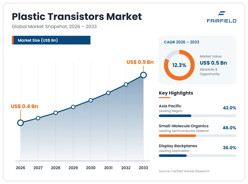
The global plastic transistors market size is expected to be valued at US$ 0.4 billion in 2026 and projected to reach US$ 0.9 billion by 2033, growing at a CAGR of 12.3% between 2026 and 2033.
The base is small and the commercial record is early. Between 2020 and 2025 the market grew at a CAGR of about 11%, moving from laboratory demonstrations into limited production use in electronic paper backplanes, large-area sensor arrays and single-use biosensors. Three factors support the forecast: low-temperature processing that builds circuits directly on plastic film, printing steps that cut tooling cost across wide areas, and demand for conformable sensing in medical and logistics settings. Progress has been slower than this field promised for two decades. Carrier mobility and operating stability still decide where organic devices can be used, so the direction of travel is steady niche adoption rather than broad replacement of silicon or metal-oxide electronics.
Key Report Takeaways
- By Semiconductor Material: Small-molecule organic semiconductors held 48% share in 2026, while polymer semiconductors are projected to expand at a 14.6% CAGR through 2033, since solution-coatable conjugated polymers suit roll-to-roll lines on thin plastic film.
- By Fabrication Process: Vacuum thermal evaporation held 45% share in 2026, while printing is projected to grow at a 15.4% CAGR through 2033, because inkjet and gravure steps remove photolithography masks from large-area patterning work.
- By Substrate: Plastic film held 58% share in 2026, while paper and textile substrates are projected to advance at a 15.8% CAGR through 2033, supported by single-use smart labels and wearable patches that tolerate modest device performance.
- By Application: Flexible display and electronic paper backplanes held 36% share in 2026, while biosensors and medical patches are projected to rise at a 16.2% CAGR through 2033, as disposable test strips match the economics of cheap printed devices.
- By Geography: Asia Pacific held 42% share in 2026, while North America is projected to record a 14.2% CAGR through 2033, helped by diagnostics demand and public funding for flexible hybrid electronics research.
Global Plastic Transistors Market Trends and Insights
Drivers Impact Analysis
Two forces account for most of the measurable demand in this market today.
| Driver | Impact on CAGR Forecast | Geographic Relevance | Impact Timeline |
| Low-temperature and printed processing on plastic film lowers large-area backplane cost | Medium | Asia Pacific, Europe | Medium term (2–4 years) |
| Single-use biosensors and skin patches suit cheap, mechanically flexible devices | Medium | North America, Europe | Long term (≥4 years) |
Low-Temperature Printing on Plastic Film Lowers Large-Area Backplane Cost
Organic semiconductors can be deposited below 150 °C, which allows transistor backplanes to be built directly on PET and PEN film rather than on glass. That single property drives most current demand, because it removes the high-temperature steps that force conventional lines onto rigid substrates. Electronic paper modules and segmented signage are the clearest beneficiaries, and both are now bought in commercial quantities.
The causal mechanism is tooling cost per unit area. Solution coating, slot-die and inkjet patterning replace vacuum deposition and photolithography masks, so a line can pattern a wide web without a mask set for each design. Roll-to-roll handling raises substrate throughput further. Public pilot-line programmes for flexible and printed electronics in the European Union, Japan and Korea fund this equipment, and the IEC printed electronics standards work supports measurement consistency across suppliers quoting the same job.
Single-Use Medical Sensing Creates Demand Organic Devices Can Serve
Disposable diagnostics are the application where organic transistor economics work, and they now account for a rising share of device shipments. A test strip or skin patch is discarded after one use, so the device never faces the multi-year stability problem that blocks organic electronics elsewhere. Low switching speed is also acceptable, since the biochemical signals being measured change slowly by comparison with digital electronics.
The mechanism is matched requirements rather than improved performance. Organic electrochemical and thin-film devices amplify small ionic and electrochemical signals directly at the skin or sample, which cuts the external circuitry needed in a disposable product. Point-of-care testing and continuous monitoring patches drive the volume. Sterile single-use packaging follows ISO 11607 and medical device requirements, and material selection follows RoHS and REACH, which suppliers of organic semiconductor inks already address.
Restraints Impact Analysis
Two long-standing technical limits explain why commercialisation has stayed partial.
| Restraint | Impact on CAGR Forecast | Geographic Relevance | Impact Timeline |
| Carrier mobility far below silicon and below metal-oxide semiconductors caps switching speed | High | Global | Long term (≥4 years) |
| Bias, heat, oxygen and moisture instability forces costly barrier encapsulation | High | Global | Long term (≥4 years) |
Carrier Mobility Below Silicon Keeps Organic Devices Out of Fast Electronics
Charge carrier mobility in organic semiconductors remains far below crystalline silicon and below amorphous metal-oxide semiconductors such as IGZO. That gap caps switching speed and drive current, so organic devices are ruled out of processors, memory controllers, high-refresh displays and radio front ends. The addressable band is narrow: applications where cost per area and bending tolerance matter more than speed.
The cause is physical. Charge transport in these films moves by hopping between weakly coupled molecules rather than through a continuous crystal lattice, and grain boundaries, molecular disorder and contact resistance each reduce effective mobility further. Record laboratory values come from small, carefully grown crystals that do not survive volume coating. Metal-oxide backplanes reached acceptable mobility at low process temperatures first, which is why they won most flexible display backplane work.
Encapsulation Needed for Stability Erodes the Cost and Flexibility Case
Operational and environmental stability is the persistent engineering problem in this field, and it directly reduces the commercial advantage. Organic films degrade under continued gate bias, elevated temperature, oxygen and moisture, so threshold voltage shifts and drive current falls during normal use. Products that must keep working for several years need protection that the bare device cannot provide on its own.
The specific cost source is the barrier stack. Multilayer thin-film encapsulation with alternating inorganic and organic layers, edge sealing and desiccant adds deposition steps, yield loss and material cost to a process chosen for being cheap. The stack also stiffens the finished part, which cuts the bend radius that justified choosing plastic film in the first place. Encapsulated organic devices therefore compete on total cost against incumbent components that need no such treatment.
Market Opportunities
Two revenue pools remain genuinely open rather than already contested.
Electronic Shelf Labels and Segmented Signage Open a Volume Backplane Pool
Low-refresh electronic paper displays are the nearest thing to a volume opportunity for organic backplanes, because they need switching only when content changes. Retail shelf labels, transport signage, logistics tags and industrial indicators replace printed cards across very large installed estates, and each installation uses thousands of small displays at low unit value but steady repeat volume.
Materials suppliers and specialist device houses can capture this pool, with display module makers as the customer group. The demand comes from retailers and logistics operators managing frequent price and routing changes across thousands of items. Supporting developments include conductive polymer and organic semiconductor ink supply from chemical producers, and the IEC TC 119 standards work on printed electronics terminology, materials and measurement methods, which gives buyers a common basis for comparing competing supplier claims.
Conformable Large-Area Sensor Arrays Open an Imaging and Pressure-Mapping Pool
Large-area sensing is the second open pool, because no silicon alternative covers wide curved surfaces at acceptable cost. Pressure-mapping mats, X-ray and image sensor panels, and conformable strain and temperature arrays all need thousands of addressing transistors spread over an area far larger than any economic silicon die, and bonding separate chips across that area costs more than the sensing itself.
Device integrators and sensor makers can capture this work, with medical imaging, physical rehabilitation, industrial inspection and robotics teams forming the customer base. The requirement is coverage and conformability rather than speed, which matches organic device capability directly. Characterisation uses ISO and IEC test methods for flexible and printed devices, and public research funding for flexible electronics in Europe, Japan and Korea continues to support the prototype lines that feed this application.
Segment Analysis
- By Semiconductor Material: Small-Molecule Films Lead While Polymers Gain Ground
Small-molecule organic semiconductors held 48% share in 2026, because vacuum-deposited films give the most uniform grain structure and the highest reproducible mobility available in volume. Device houses building electronic paper backplanes favour them for yield rather than for cost, since evaporation equipment is well understood and film thickness is tightly controlled.
Polymer semiconductors are the fastest-growing material at a 14.6% CAGR through 2033. Conjugated polymers dissolve in common solvents, so they can be slot-die coated or printed on moving web, which suits the roll-to-roll ambition of this sector. Formulation work by chemical suppliers has narrowed the mobility gap with small molecules while improving shelf life of the ink.
Hybrid blends combining small molecules with polymer binders sit between the two and are used where coating uniformity matters more than peak performance. The business implication is that material choice now follows the intended process route rather than the application.
- By Fabrication Process: Evaporation Holds Volume While Printing Expands Fastest
Vacuum thermal evaporation held 45% share in 2026, since it remains the route with proven yield for commercial organic thin-film transistor backplanes. Lines already installed for organic light-emitting diode production transfer to this work with modest change, which keeps capital cost contained for existing manufacturers.
Printing is the fastest-growing process at a 15.4% CAGR through 2033. Inkjet, screen and gravure patterning remove the mask sets that dominate large-area tooling cost, and additive deposition wastes less material than subtractive patterning. Printed layers also tolerate wide, thin substrates that would crack under conventional handling.
Solution coating without patterning sits between the two and is widely used for dielectric and interface layers. The implication for buyers is that printed device performance still trails evaporated performance, so process choice remains a direct trade between unit cost and achievable mobility in the finished circuit.
- By Substrate: Plastic Film Dominates While Paper and Textile Grow Quickest
Plastic film held 58% share in 2026, because PET and PEN webs combine dimensional stability, surface smoothness and chemical resistance at low cost. Smoothness matters directly, since surface roughness disrupts the thin semiconducting channel and lowers device yield across a wide panel.
Paper and textile substrates are the fastest-growing group at a 15.8% CAGR through 2033. Single-use smart packaging labels and wearable patches accept lower device performance and shorter life, which suits a cheap porous substrate. Coating and planarisation layers have improved enough to make printed devices on these materials repeatable.
Glass remains in use for development, pilot work and some rigid electronic paper modules where flexibility is not required. The implication is that substrate choice now sets the realistic ceiling on device performance before the semiconductor is even selected, which shapes how suppliers quote projects.
- By Application: Electronic Paper Backplanes Lead While Biosensors Accelerate
Flexible display and electronic paper backplanes held 36% share in 2026, the largest single use, because low-refresh displays tolerate slow switching and reward low cost per unit area. Shelf labels, transport signage and reader panels together give the only steady production volume this technology has achieved.
Biosensors and medical patches are the fastest-growing application at a 16.2% CAGR through 2033. Disposable use removes the stability problem, and direct electrochemical signal amplification reduces external components in a low-value product. Point-of-care diagnostics and continuous monitoring patches drive the demand.
Large-area and conformable sensor arrays, radio-frequency identification and near-field tags, flexible logic and research prototyping make up the remainder. Printed tags are the weakest of these, since silicon chip prices fell faster than printed device performance improved. The implication is that growth concentrates where single use or wide area defeats silicon economics.
Geography Analysis
- Which Region Is Growing Fastest in the Plastic Transistors Market?
North America is the fastest-growing region at a 14.2% CAGR through 2033, from 23% share in 2026, and medical sensing explains most of that growth. Diagnostics companies and device start-ups in the United States treat disposable electrochemical sensing as the clearest commercial route for organic devices, and the regulatory route for single-use sensing products is already familiar to them.
Public funding for flexible hybrid electronics research and shared pilot facilities has supported prototype lines and workforce skills, while university groups continue to publish the material advances that suppliers later commercialise. Canada adds printable electronics research capacity. The barrier is volume manufacturing: the region prototypes well but sends most production work to established panel and module makers elsewhere, which caps the value captured locally.
- Europe Anchors Materials Supply and Pilot-Line Capacity for Organic Circuits
Europe held 26% share in 2026, second largest, and its position rests on chemistry and shared pilot facilities rather than on display volume. Germany, the United Kingdom, the Netherlands and Belgium host the specialty material suppliers, equipment builders and open-access pilot lines that most organic device developers use at some stage.
Regulatory discipline shapes material selection, since RoHS and REACH compliance governs the solvents, dopants and metals permitted in commercial inks. The region also carries much of the standardisation effort through IEC committee work on printed electronics. Public research programmes fund flexible electronics pilot lines across several member states. The main change shaping the region is a shift of funding emphasis from demonstrator projects toward qualification work that manufacturers can actually buy against.
- Which Region Is Leading the Plastic Transistors Market?
Asia Pacific leads with 42% share in 2026, because the display and specialty chemical supply chains that organic devices depend on are concentrated there. Japan supplies much of the organic semiconductor and dielectric material used worldwide, while Korea, Taiwan and China hold the panel, module and electronic paper assembly capacity that turns backplanes into products.
Proximity matters in this market. Material suppliers, equipment builders and module assemblers sit close enough to iterate quickly on coating recipes and encapsulation stacks, which shortens qualification cycles that otherwise run for years. National research programmes in Japan and Korea continue to fund printed and flexible electronics pilot work. The opportunity shaping the region is electronic paper demand from retail and logistics, which gives local module makers their first repeatable production volume.
- Latin America Remains an Import-Led Market for Flexible Electronic Components
Latin America held 5% share in 2026, a small position built on imported modules rather than local device fabrication. Brazil and Mexico account for most of it, through electronics assembly plants and retail chains adopting electronic shelf labels in larger store formats.
The barriers are structural. No commercial organic transistor fabrication capacity exists in the region, specialty semiconductor inks must be imported with long lead times, and customs and currency exposure raise the delivered cost of low-value devices where margin is thin. Research activity is confined to a handful of university groups. The change worth watching is retail electronic labelling, which gives suppliers a defined, repeatable product to sell without requiring any local manufacturing investment at all.
- Middle East & Africa Builds Research Capacity Ahead of Commercial Demand
Middle East & Africa held 4% share in 2026, the smallest regional position, and demand is concentrated in a few national research programmes rather than in production. Israel, the United Arab Emirates and Saudi Arabia fund flexible and printed electronics work inside universities and new research institutes.
The barriers are a thin local supply chain and no panel or module manufacturing base, so every material and tool is imported and skilled process staff are scarce. Commercial uptake is limited to imported electronic shelf labels and signage in modern retail. The opportunity is tied to diversification programmes that fund advanced materials research, which can seed small specialist suppliers even while volume device manufacturing stays outside the region for the foreseeable period.
Competitive Landscape
The market is highly fragmented and has low concentration, which is typical of a technology that has not reached volume production. No single company controls the chain from semiconductor ink to finished flexible circuit. Specialty chemical producers supply the organic semiconductors, dielectrics and conductive polymers; a small group of technology developers licenses device and process know-how; and display or sensor module makers integrate the result. Several early device companies have exited or redirected toward adjacent products, which has thinned the field rather than consolidated it.
Competition rests on material performance and process compatibility rather than on price. Buyers compare carrier mobility under realistic coating conditions, threshold voltage stability under bias and heat, ink shelf life, and whether a formulation runs on equipment they already own. Encapsulation capability is a decisive factor, since a device that cannot be protected economically has no product. New entrants mostly arrive from chemistry rather than semiconductors, and a second group of entrants comes from biosensing, where organic electrochemical devices are being designed into disposable diagnostic formats.
Strategic activity concentrates on partnerships between material suppliers and pilot-line operators, on licensing device architectures to module manufacturers, and on qualification work with named end customers in electronic paper and sensing. These arrangements matter because no participant can afford a dedicated volume line before demand is proven, so shared pilot capacity substitutes for owned capacity. Public research programmes supply much of the funding behind this work.
Vendor strategy is shifting from demonstration toward qualification. Suppliers now target applications where single use or large area removes the comparison with silicon, and present organic devices as complements to metal-oxide and silicon electronics rather than as replacements for them.
Recent Industry Developments
- July 2024: The European Union’s Ecodesign for Sustainable Products Regulation entered into force, extending durability, repairability and digital product passport requirements toward electronic goods – raising the compliance bar for materials used in flexible and printed devices sold in Europe.
- December 2024: The European Union’s General Product Safety Regulation became applicable to consumer products placed on the market – adding traceability and safety documentation duties that reach suppliers of novel electronic components sold into consumer applications.
- February 2025: The European Union’s Packaging and Packaging Waste Regulation entered into force, tightening recyclability and material requirements for packaging – a direct constraint on how printed tags and smart labels are attached to and separated from consumer packaging.
Companies Covered in the Report
- Merck KGaA
- Sumitomo Chemical Co., Ltd.
- BASF SE
- Mitsubishi Chemical Group Corporation
- Nissan Chemical Corporation
- JSR Corporation
- Toray Industries, Inc.
- Heraeus Holding GmbH
- Agfa-Gevaert NV
- FlexEnable Limited
- SmartKem, Inc.
- Flexterra, Inc.
- E Ink Holdings Inc.
Plastic Transistors Market Report Scope
| Metric | Value |
| Study Period | 2020–2033 |
| Market Size 2026 | US$ 0.4 Billion |
| Market Size 2033 | US$ 0.9 Billion |
| CAGR 2026–2033 | 12.3% |
| Absolute Dollar Opportunity | US$ 0.5 Billion |
| Largest Market | Asia Pacific (42% share in 2026) |
| Fastest-Growing Market | North America (14.2% CAGR) |
| Market Concentration | Low |
| Major Players | Merck KGaA, Sumitomo Chemical, FlexEnable, Nissan Chemical Corporation, Heraeus Holding |
Plastic Transistors Market Segmentation
Semiconductor Material
- Small-Molecule Organic Semiconductors
- Polymer Semiconductors
- Hybrid Blends
Fabrication Process
- Vacuum Thermal Evaporation
- Solution Coating
- Printing
Substrate
- Plastic Film
- Glass
- Paper and Textile
Application
- Flexible Display and Electronic Paper Backplanes
- Large-Area and Conformable Sensor Arrays
- Biosensors and Medical Patches
- Radio-Frequency Identification and Near-Field Tags
- Flexible Logic and Research Prototyping
Regions
- North America
- Europe
- Asia Pacific
- Latin America
- Middle East & Africa
- Executive Summary
- Global Plastic Transistors Market Snapshot
- Future Projections, 2026-2033
- Key Market Trends
- Regional Snapshot
- Market Overview
- Market Definition and Report Scope
- Historical Market Trends, 2020-2025
- Market Dynamics
- Drivers Impact Analysis
- Low-Temperature Printing on Plastic Film Lowers Large-Area Backplane Cost
- Single-Use Medical Sensing Creates Demand Organic Devices Can Serve
- Restraints Impact Analysis
- Carrier Mobility Below Silicon Keeps Organic Devices Out of Fast Electronics
- Encapsulation Needed for Stability Erodes the Cost and Flexibility Case
- Market Opportunities
- Electronic Shelf Labels and Segmented Signage Open a Volume Backplane Pool
- Conformable Large-Area Sensor Arrays Open an Imaging and Pressure-Mapping Pool
- Drivers Impact Analysis
- Global Plastic Transistors Market Outlook, 2020-2033
- Global Plastic Transistors Market Outlook, by Semiconductor Material, Value (US$ Billion), 2020-2033
- Small-Molecule Organic Semiconductors
- Polymer Semiconductors
- Hybrid Blends
- Global Plastic Transistors Market Outlook, by Fabrication Process, Value (US$ Billion), 2020-2033
- Vacuum Thermal Evaporation
- Solution Coating
- Printing
- Global Plastic Transistors Market Outlook, by Substrate, Value (US$ Billion), 2020-2033
- Plastic Film
- Glass
- Paper and Textile
- Global Plastic Transistors Market Outlook, by Application, Value (US$ Billion), 2020-2033
- Flexible Display and Electronic Paper Backplanes
- Large-Area and Conformable Sensor Arrays
- Biosensors and Medical Patches
- Radio-Frequency Identification and Near-Field Tags
- Flexible Logic and Research Prototyping
- Global Plastic Transistors Market Outlook, by Region, Value (US$ Billion), 2020-2033
- North America
- Europe
- Asia Pacific
- Latin America
- Middle East & Africa
- Global Plastic Transistors Market Outlook, by Semiconductor Material, Value (US$ Billion), 2020-2033
- North America Plastic Transistors Market Outlook, 2020-2033
- North America Plastic Transistors Market Outlook, by Semiconductor Material, Value (US$ Billion), 2020-2033
- Small-Molecule Organic Semiconductors
- Polymer Semiconductors
- Hybrid Blends
- North America Plastic Transistors Market Outlook, by Fabrication Process, Value (US$ Billion), 2020-2033
- Vacuum Thermal Evaporation
- Solution Coating
- Printing
- North America Plastic Transistors Market Outlook, by Substrate, Value (US$ Billion), 2020-2033
- Plastic Film
- Glass
- Paper and Textile
- North America Plastic Transistors Market Outlook, by Application, Value (US$ Billion), 2020-2033
- Flexible Display and Electronic Paper Backplanes
- Large-Area and Conformable Sensor Arrays
- Biosensors and Medical Patches
- Radio-Frequency Identification and Near-Field Tags
- Flexible Logic and Research Prototyping
- North America Plastic Transistors Market Outlook, by Country, Value (US$ Billion), 2020-2033
- United States Plastic Transistors Market Outlook, by Semiconductor Material, 2020-2033
- United States Plastic Transistors Market Outlook, by Fabrication Process, 2020-2033
- United States Plastic Transistors Market Outlook, by Substrate, 2020-2033
- United States Plastic Transistors Market Outlook, by Application, 2020-2033
- Canada Plastic Transistors Market Outlook, by Semiconductor Material, 2020-2033
- Canada Plastic Transistors Market Outlook, by Fabrication Process, 2020-2033
- Canada Plastic Transistors Market Outlook, by Substrate, 2020-2033
- Canada Plastic Transistors Market Outlook, by Application, 2020-2033
- North America Plastic Transistors Market Outlook, by Semiconductor Material, Value (US$ Billion), 2020-2033
- Europe Plastic Transistors Market Outlook, 2020-2033
- Europe Plastic Transistors Market Outlook, by Semiconductor Material, Value (US$ Billion), 2020-2033
- Small-Molecule Organic Semiconductors
- Polymer Semiconductors
- Hybrid Blends
- Europe Plastic Transistors Market Outlook, by Fabrication Process, Value (US$ Billion), 2020-2033
- Vacuum Thermal Evaporation
- Solution Coating
- Printing
- Europe Plastic Transistors Market Outlook, by Substrate, Value (US$ Billion), 2020-2033
- Plastic Film
- Glass
- Paper and Textile
- Europe Plastic Transistors Market Outlook, by Application, Value (US$ Billion), 2020-2033
- Flexible Display and Electronic Paper Backplanes
- Large-Area and Conformable Sensor Arrays
- Biosensors and Medical Patches
- Radio-Frequency Identification and Near-Field Tags
- Flexible Logic and Research Prototyping
- Europe Plastic Transistors Market Outlook, by Country, Value (US$ Billion), 2020-2033
- Germany Plastic Transistors Market Outlook, by Semiconductor Material, 2020-2033
- Germany Plastic Transistors Market Outlook, by Fabrication Process, 2020-2033
- Germany Plastic Transistors Market Outlook, by Substrate, 2020-2033
- Germany Plastic Transistors Market Outlook, by Application, 2020-2033
- United Kingdom Plastic Transistors Market Outlook, by Semiconductor Material, 2020-2033
- United Kingdom Plastic Transistors Market Outlook, by Fabrication Process, 2020-2033
- United Kingdom Plastic Transistors Market Outlook, by Substrate, 2020-2033
- United Kingdom Plastic Transistors Market Outlook, by Application, 2020-2033
- Netherlands Plastic Transistors Market Outlook, by Semiconductor Material, 2020-2033
- Netherlands Plastic Transistors Market Outlook, by Fabrication Process, 2020-2033
- Netherlands Plastic Transistors Market Outlook, by Substrate, 2020-2033
- Netherlands Plastic Transistors Market Outlook, by Application, 2020-2033
- Belgium Plastic Transistors Market Outlook, by Semiconductor Material, 2020-2033
- Belgium Plastic Transistors Market Outlook, by Fabrication Process, 2020-2033
- Belgium Plastic Transistors Market Outlook, by Substrate, 2020-2033
- Belgium Plastic Transistors Market Outlook, by Application, 2020-2033
- Europe Plastic Transistors Market Outlook, by Semiconductor Material, Value (US$ Billion), 2020-2033
- Asia Pacific Plastic Transistors Market Outlook, 2020-2033
- Asia Pacific Plastic Transistors Market Outlook, by Semiconductor Material, Value (US$ Billion), 2020-2033
- Small-Molecule Organic Semiconductors
- Polymer Semiconductors
- Hybrid Blends
- Asia Pacific Plastic Transistors Market Outlook, by Fabrication Process, Value (US$ Billion), 2020-2033
- Vacuum Thermal Evaporation
- Solution Coating
- Printing
- Asia Pacific Plastic Transistors Market Outlook, by Substrate, Value (US$ Billion), 2020-2033
- Plastic Film
- Glass
- Paper and Textile
- Asia Pacific Plastic Transistors Market Outlook, by Application, Value (US$ Billion), 2020-2033
- Flexible Display and Electronic Paper Backplanes
- Large-Area and Conformable Sensor Arrays
- Biosensors and Medical Patches
- Radio-Frequency Identification and Near-Field Tags
- Flexible Logic and Research Prototyping
- Asia Pacific Plastic Transistors Market Outlook, by Country, Value (US$ Billion), 2020-2033
- Japan Plastic Transistors Market Outlook, by Semiconductor Material, 2020-2033
- Japan Plastic Transistors Market Outlook, by Fabrication Process, 2020-2033
- Japan Plastic Transistors Market Outlook, by Substrate, 2020-2033
- Japan Plastic Transistors Market Outlook, by Application, 2020-2033
- Korea Plastic Transistors Market Outlook, by Semiconductor Material, 2020-2033
- Korea Plastic Transistors Market Outlook, by Fabrication Process, 2020-2033
- Korea Plastic Transistors Market Outlook, by Substrate, 2020-2033
- Korea Plastic Transistors Market Outlook, by Application, 2020-2033
- Taiwan Plastic Transistors Market Outlook, by Semiconductor Material, 2020-2033
- Taiwan Plastic Transistors Market Outlook, by Fabrication Process, 2020-2033
- Taiwan Plastic Transistors Market Outlook, by Substrate, 2020-2033
- Taiwan Plastic Transistors Market Outlook, by Application, 2020-2033
- China Plastic Transistors Market Outlook, by Semiconductor Material, 2020-2033
- China Plastic Transistors Market Outlook, by Fabrication Process, 2020-2033
- China Plastic Transistors Market Outlook, by Substrate, 2020-2033
- China Plastic Transistors Market Outlook, by Application, 2020-2033
- Asia Pacific Plastic Transistors Market Outlook, by Semiconductor Material, Value (US$ Billion), 2020-2033
- Latin America Plastic Transistors Market Outlook, 2020-2033
- Latin America Plastic Transistors Market Outlook, by Semiconductor Material, Value (US$ Billion), 2020-2033
- Small-Molecule Organic Semiconductors
- Polymer Semiconductors
- Hybrid Blends
- Latin America Plastic Transistors Market Outlook, by Fabrication Process, Value (US$ Billion), 2020-2033
- Vacuum Thermal Evaporation
- Solution Coating
- Printing
- Latin America Plastic Transistors Market Outlook, by Substrate, Value (US$ Billion), 2020-2033
- Plastic Film
- Glass
- Paper and Textile
- Latin America Plastic Transistors Market Outlook, by Application, Value (US$ Billion), 2020-2033
- Flexible Display and Electronic Paper Backplanes
- Large-Area and Conformable Sensor Arrays
- Biosensors and Medical Patches
- Radio-Frequency Identification and Near-Field Tags
- Flexible Logic and Research Prototyping
- Latin America Plastic Transistors Market Outlook, by Country, Value (US$ Billion), 2020-2033
- Brazil Plastic Transistors Market Outlook, by Semiconductor Material, 2020-2033
- Brazil Plastic Transistors Market Outlook, by Fabrication Process, 2020-2033
- Brazil Plastic Transistors Market Outlook, by Substrate, 2020-2033
- Brazil Plastic Transistors Market Outlook, by Application, 2020-2033
- Mexico Plastic Transistors Market Outlook, by Semiconductor Material, 2020-2033
- Mexico Plastic Transistors Market Outlook, by Fabrication Process, 2020-2033
- Mexico Plastic Transistors Market Outlook, by Substrate, 2020-2033
- Mexico Plastic Transistors Market Outlook, by Application, 2020-2033
- Latin America Plastic Transistors Market Outlook, by Semiconductor Material, Value (US$ Billion), 2020-2033
- Middle East & Africa Plastic Transistors Market Outlook, 2020-2033
- Middle East & Africa Plastic Transistors Market Outlook, by Semiconductor Material, Value (US$ Billion), 2020-2033
- Small-Molecule Organic Semiconductors
- Polymer Semiconductors
- Hybrid Blends
- Middle East & Africa Plastic Transistors Market Outlook, by Fabrication Process, Value (US$ Billion), 2020-2033
- Vacuum Thermal Evaporation
- Solution Coating
- Printing
- Middle East & Africa Plastic Transistors Market Outlook, by Substrate, Value (US$ Billion), 2020-2033
- Plastic Film
- Glass
- Paper and Textile
- Middle East & Africa Plastic Transistors Market Outlook, by Application, Value (US$ Billion), 2020-2033
- Flexible Display and Electronic Paper Backplanes
- Large-Area and Conformable Sensor Arrays
- Biosensors and Medical Patches
- Radio-Frequency Identification and Near-Field Tags
- Flexible Logic and Research Prototyping
- Middle East & Africa Plastic Transistors Market Outlook, by Country, Value (US$ Billion), 2020-2033
- Israel Plastic Transistors Market Outlook, by Semiconductor Material, 2020-2033
- Israel Plastic Transistors Market Outlook, by Fabrication Process, 2020-2033
- Israel Plastic Transistors Market Outlook, by Substrate, 2020-2033
- Israel Plastic Transistors Market Outlook, by Application, 2020-2033
- United Arab Emirates Plastic Transistors Market Outlook, by Semiconductor Material, 2020-2033
- United Arab Emirates Plastic Transistors Market Outlook, by Fabrication Process, 2020-2033
- United Arab Emirates Plastic Transistors Market Outlook, by Substrate, 2020-2033
- United Arab Emirates Plastic Transistors Market Outlook, by Application, 2020-2033
- Saudi Arabia Plastic Transistors Market Outlook, by Semiconductor Material, 2020-2033
- Saudi Arabia Plastic Transistors Market Outlook, by Fabrication Process, 2020-2033
- Saudi Arabia Plastic Transistors Market Outlook, by Substrate, 2020-2033
- Saudi Arabia Plastic Transistors Market Outlook, by Application, 2020-2033
- Middle East & Africa Plastic Transistors Market Outlook, by Semiconductor Material, Value (US$ Billion), 2020-2033
- Competitive Landscape
- Market Concentration and Industry Leaders
- Competitive Differentiation
- Strategic Initiatives
- Recent Industry Developments
- Company Profiles
- Merck KGaA
- Sumitomo Chemical Co., Ltd.
- BASF SE
- Mitsubishi Chemical Group Corporation
- Nissan Chemical Corporation
- JSR Corporation
- Toray Industries, Inc.
- Heraeus Holding GmbH
- Agfa-Gevaert NV
- FlexEnable Limited
- SmartKem, Inc.
- Flexterra, Inc.
- E Ink Holdings Inc.
- Appendix
- Research Methodology
- Report Assumptions
- Acronyms and Abbreviations
Semiconductor Material
- Small-Molecule Organic Semiconductors
- Polymer Semiconductors
- Hybrid Blends
Fabrication Process
- Vacuum Thermal Evaporation
- Solution Coating
- Printing
Substrate
- Plastic Film
- Glass
- Paper and Textile
Application
- Flexible Display and Electronic Paper Backplanes
- Large-Area and Conformable Sensor Arrays
- Biosensors and Medical Patches
- Radio-Frequency Identification and Near-Field Tags
- Flexible Logic and Research Prototyping
Regions
- North America
- Europe
- Asia Pacific
- Latin America
- Middle East & Africa
Our Research Methodology
Considering the volatility of business today, traditional approaches to strategizing a game plan can be unfruitful if not detrimental. True ambiguity is no way to determine a forecast. A myriad of predetermined factors must be accounted for such as the degree of risk involved, the magnitude of circumstances, as well as conditions or consequences that are not known or unpredictable. To circumvent binary views that cast uncertainty, the application of market research intelligence to strategically posture, move, and enable actionable outcomes is necessary.
View Methodology
Quality Assured
Rigorous Validation Process

Confidentiality Assured
End-to-end Data Security

Custom Research Services
Tailored To Your Objectives
FAQs
The market is valued at US$ 0.4 billion in 2026, a deliberately small base that reflects limited production use outside electronic paper and disposable sensing.
The market is projected to reach US$ 0.9 billion by 2033, growing at a 12.3% CAGR and adding US$ 0.5 billion over the forecast period.
Flexible display and electronic paper backplanes hold 36% share in 2026, the only application with steady repeatable production volume today.
Biosensors and medical patches grow fastest at a 16.2% CAGR, while North America leads regional growth at a 14.2% CAGR through 2033.
Asia Pacific leads with 42% share in 2026, and concentration is low, with materials, device and module suppliers spread across many small participants.
Related Reports
Multi-Access Edge Computing Market Size, Share, Insights, Competitive Landscape, and Forecast 2026 to 2033
Explore the multi-access edge computing market, valued at US$ 4.2 billion in 2026 and projected to reach US$ 9.8 billion by 2033 at a 12.9% CAGR.
M-commerce Payment Market Size, Share, Insights, Competitive Landscape, and Forecast 2026 to 2033
Explore the m-commerce payment market, valued at US$ 10.05 billion in 2026 and forecast to reach US$ 22.70 billion by 2033, growing at a 12.3% CAGR.
Irrigation Automation Market Size, Share, Insights, Competitive Landscape, and Forecast 2026 to 2033
Irrigation automation market to grow from US$ 6.2 billion in 2026 to US$ 18.5 billion by 2033 at a 16.9% CAGR. Explore components, end users and regional trends.
Underwater LiDAR Market Size, Share, Insights, Competitive Landscape, and Forecast 2026 to 2033
Explore the underwater LiDAR market, projected to reach US$0.9 billion by 2033 at 12.3% CAGR, with platform, application and regional insights.
Aerial Imaging Market Size, Share, Insights, Competitive Landscape, and Forecast 2026 to 2033
The global aerial imaging market is valued at US$3.83 billion in 2026, reaching US$8.13 billion by 2033, growing at an 11.4% CAGR
Satcom Terminal Market Size, Share, Insights, Competitive Landscape, and Forecast 2026 to 2033
The satcom terminal market is projected to grow from US$8.6 billion in 2026 to US$20.6 billion by 2033, at a 13.3% CAGR. Explore segments and key trends.