



3D IC and 2.5D IC Packaging Market
3D IC and 2.5D IC Packaging Market Size, Share, Insights, Competitive Landscape, and Forecast 2026 to 2033
3D IC and 2.5D IC Packaging Market Size and Trend Analysis
How Fast Is the 3D IC and 2.5D IC Packaging Market Growing?
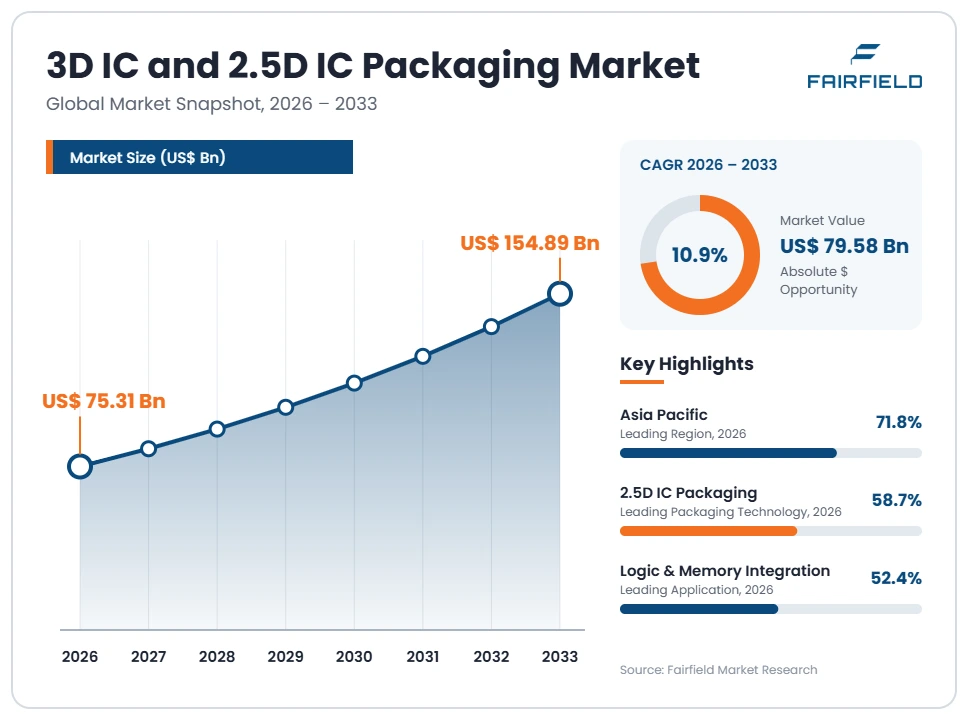
The global 3D IC and 2.5D IC packaging market size is expected to be valued at US$ 75.31 billion in 2026 and projected to reach US$ 154.89 billion by 2033, growing at a CAGR of 10.9% between 2026 and 2033.
Between 2020 and 2025, the market grew at a CAGR of about 13.2%, as demand for high-performance computing chips and high-bandwidth memory surged with the rise of generative AI. Three factors now drive growth: AI accelerators that combine large logic dies with stacked HBM memory, the move to chiplet architectures as transistor scaling slows, and government support for domestic advanced packaging. The market is shifting from conventional flip-chip packages toward silicon interposers, hybrid bonding, and through-silicon via stacks that deliver higher bandwidth and better power efficiency.
Key Report Takeaways
- By Packaging Technology: 2.5D IC Packaging held 58.7% share in 2026, while 3D IC Packaging is projected to expand at a 13.4% CAGR through 2033, driven by hybrid bonding and stacked logic-on-logic designs.
- By Interconnect Technology: Through-Silicon Via held 44.2% share in 2026, while Hybrid Bonding is projected to expand at a 24.8% CAGR through 2033, driven by finer pitches needed for HBM4 and stacked processors.
- By Application: Logic & Memory Integration held 52.4% share in 2026, while AI & High-Performance Computing Accelerators are projected to expand at a 16.3% CAGR through 2033, driven by data center investment in generative AI.
- By End-user Industry: Consumer Electronics held 36.5% share in 2026, while Data Center & IT is projected to expand at a 15.7% CAGR through 2033, driven by hyperscale AI clusters.
- By Region: Asia Pacific held 71.8% share in 2026, while North America is projected to expand at a 17.6% CAGR through 2033, driven by new packaging plants in Arizona and Indiana supported by the CHIPS and Science Act.
Global 3D IC and 2.5D IC Packaging Market Trends and Insights
Drivers Impact Analysis
Two drivers carry the strongest influence on 3D IC and 2.5D IC packaging demand during the forecast period.
| Driver | Impact on CAGR Forecast | Geographic Relevance | Impact Timeline |
| AI accelerator and HBM demand | High | Global, strongest in Asia Pacific and North America | Short term (≤2 years) |
| Chiplet adoption as transistor scaling slows | High | Global | Long term (≥4 years) |
AI Accelerators and HBM Are Driving 3D IC and 2.5D IC Packaging Demand
AI accelerators and high-bandwidth memory are the strongest drivers of 3D IC and 2.5D IC packaging demand. Graphics processors and custom AI chips need huge memory bandwidth, which can only be delivered by placing stacked memory right next to the processor.
The mechanism is advanced packaging integration. In 2.5D designs, processors and HBM stacks sit side by side on a silicon interposer with thousands of fine connections. HBM itself is a 3D stack of memory dies connected by through-silicon vias. TSMC’s CoWoS technology is used for many leading AI chips, and supply has been tight. Reports in June 2026 indicated the CoWoS supply-demand gap was expected to narrow from about 20% to 10% by the end of 2026 as new capacity came online. CoWoS wafer prices were reported near US$ 10,000 per wafer, showing the high value of these packages.
Chiplet Architectures Are Expanding 3D IC and 2.5D IC Packaging Use
Chiplet architectures are expanding the use of 3D IC and 2.5D IC packaging beyond AI. As shrinking transistors becomes slower and more expensive, chip designers split large chips into smaller dies and connect them in a single package.
The cause is the rising cost of advanced manufacturing nodes. Large monolithic dies have lower yields and higher costs at leading nodes. Chiplets let companies use the most advanced process only where needed and reuse proven dies for input-output and memory functions. AMD, Intel, and Apple already use chiplet or multi-die designs in processors. Design software from companies such as Siemens, which launched Innovator3D IC in June 2024, and Cadence, which acquired Invecas in January 2024, supports multi-die design. These trends extend packaging demand to servers, PCs, networking, and automotive chips.
Restraints Impact Analysis
Two restraints limit how quickly 3D IC and 2.5D IC packaging capacity can grow.
| Restraint | Impact on CAGR Forecast | Geographic Relevance | Impact Timeline |
| Thermal management and yield challenges | High | Global | Medium term (2–4 years) |
| High capital cost and supply chain concentration | Medium | Asia Pacific, North America | Medium term (2–4 years) |
Thermal and Yield Challenges Limit 3D IC and 2.5D IC Packaging
Thermal management and yield challenges limit how fast 3D IC and 2.5D IC packaging can scale. Stacking dies and placing many chips close together concentrates heat and increases the risk of defects.
The underlying causes are physics and manufacturing complexity. Heat from lower dies in a 3D stack has difficulty escaping, which can reduce performance and reliability. AI packages draw more than 1,000 watts in some cases, requiring advanced cooling such as liquid cooling. Through-silicon vias and fine-pitch bonds must be precisely aligned, and a single defect can ruin an expensive package containing several costly dies. Warpage of large interposers and substrates also causes failures. Testing each die before assembly to confirm it is a known good die adds further cost. These challenges raise production costs and limit yields, especially for the largest AI packages.
High Capital Costs and Supply Concentration Constrain 3D IC and 2.5D IC Packaging
High capital costs and concentrated supply constrain the 3D IC and 2.5D IC packaging market. Building advanced packaging lines requires expensive equipment and cleanrooms, and much of the world’s capacity sits in a few locations.
The specific causes are equipment costs, skilled labor, and geography. Hybrid bonding tools, lithography for interposers, and advanced testing equipment cost millions of dollars each. Capacity for leading 2.5D packaging is heavily concentrated in Taiwan, creating supply risk for chip designers worldwide. Shortages of substrates and interposers have repeatedly delayed product launches. Packaging firms in Taiwan have raised prices; reports in July 2026 indicated ASE increased advanced packaging quotes by more than 20%. Smaller chip designers and start-ups often struggle to secure capacity, which pushes them toward alternative packaging approaches or delays their products.
Market Opportunities
Onshore Advanced Packaging Opens a New Revenue Pool in North America
Building advanced packaging capacity in North America opens a large new revenue pool for 3D IC and 2.5D IC packaging. Chip designers and governments want to reduce dependence on overseas packaging for AI and defense chips.
Packaging companies and foundries investing in the United States can capture this demand. In March 2025, TSMC announced an additional US$ 100 billion investment in Arizona, including two advanced packaging facilities. In October 2025, Amkor Technology broke ground on a US$ 7 billion packaging and test campus in Peoria, Arizona, with Apple and NVIDIA as customers. In June 2026, TSMC and Amkor signed a 10-year agreement to expand advanced packaging and testing in the United States. Chip designers, hyperscalers, and defense agencies are the main customers for onshore packaging capacity.
Hybrid Bonding and Panel-Level Packaging Create a Next-Generation Revenue Pool
Hybrid bonding and panel-level packaging create a next-generation revenue pool for 3D IC and 2.5D IC packaging. These technologies allow finer connections, larger packages, and lower cost per unit area.
Equipment makers, foundries, and memory makers can capture this opportunity. Hybrid bonding directly joins copper pads without any solder bumps, enabling connection pitches below 10 micrometers. Memory makers are evaluating hybrid bonding for future HBM generations with more stacked dies. Panel-level packaging uses large rectangular panels instead of round wafers, increasing the number of packages per batch and reducing cost for large AI chips. Glass substrates are also being developed for flatter, more dimensionally stable packages. Foundries, memory makers, and equipment suppliers such as Applied Materials, BE Semiconductor Industries, and EV Group are key participants.
Segment Analysis
- By Packaging Technology: 2.5D IC Packaging Leads While 3D IC Packaging Grows Fastest
2.5D IC Packaging held 58.7% share in 2026. Silicon interposer and bridge-based designs, such as TSMC’s CoWoS and Intel’s EMIB, are widely used for AI accelerators that combine processors and HBM. These approaches are proven, well characterized, and in high-volume production at several suppliers.
3D IC Packaging is the fastest-growing technology, expanding at a 13.4% CAGR through 2033. True 3D stacking places dies on top of each other, shortening connections and reducing power use. TSMC’s SoIC, Intel’s Foveros, and AMD’s stacked cache designs show how 3D integration is moving into mainstream products. HBM memory itself relies on 3D stacking. For the broader market, 3D growth increases demand for hybrid bonding, thermal solutions, and advanced test equipment.
- By Interconnect Technology: Through-Silicon Via Leads While Hybrid Bonding Grows Fastest
Through-Silicon Via held 44.2% share in 2026. Vertical connections through silicon dies are essential for HBM memory stacks, image sensors, and many 3D IC designs. The technology is mature and used in very high volumes by memory makers and image sensor producers.
Hybrid Bonding is the fastest-growing interconnect technology, expanding at a 24.8% CAGR through 2033. It joins copper pads directly without solder, allowing much finer pitch and higher connection density. Memory makers are preparing hybrid bonding for future HBM, and logic stacks already use it in some processors. Micro-bump and interposer-based interconnects also remain widely used in today’s 2.5D packages. For the market, hybrid bonding growth drives demand for new bonding equipment and cleaner manufacturing environments.
- By Application: Logic & Memory Integration Leads While AI & HPC Accelerators Grow Fastest
Logic & Memory Integration held 52.4% share in 2026. Placing memory close to processors improves bandwidth and reduces power use in servers, graphics cards, and high-end mobile chips. HBM-based packages for graphics and AI form a large part of this segment.
AI & High-Performance Computing Accelerators are the fastest-growing application, expanding at a 16.3% CAGR through 2033. Cloud providers and AI companies are deploying large clusters of accelerators for training and inference. Each accelerator uses large 2.5D packages with multiple HBM stacks. Custom AI chips from hyperscalers add demand. Image sensors, RF modules, and networking chips also use advanced packaging. For the market, AI accelerator growth makes data centers the most valuable customer group for packaging suppliers.
- By End-user Industry: Consumer Electronics Leads While Data Center & IT Grows Fastest
Consumer Electronics held 36.5% share in 2026. Smartphones, tablets, and PCs use 3D stacked image sensors, memory stacks, and advanced processor packages. High shipment volumes keep consumer electronics the largest end-user industry by value, even though each package is relatively low in price.
Data Center & IT is the fastest-growing end-user industry, expanding at a 15.7% CAGR through 2033. Hyperscale cloud providers are investing hundreds of billions of dollars in AI infrastructure, and each server uses high-value accelerators and memory packages. Networking switches and co-packaged optical interconnects also adopt advanced packaging. Telecommunications, automotive, and aerospace and defense are important growing users. For the market, data center growth shifts value toward large, complex packages with very high selling prices.
Geography Analysis
- Which Region Is Growing Fastest in the 3D IC and 2.5D IC Packaging Market?
North America is growing fastest in the 3D IC and 2.5D IC packaging market at a 17.6% CAGR through 2033. The CHIPS and Science Act supports new packaging capacity. TSMC announced two advanced packaging facilities in Arizona as part of a US$ 100 billion expansion, and Amkor broke ground on a US$ 7 billion campus in Peoria. SK hynix is building an HBM packaging plant in Indiana. Intel operates advanced packaging in Arizona and New Mexico. NVIDIA, AMD, Broadcom, and hyperscalers drive strong demand. One opportunity is secure packaging for defense and government chips.
- Europe Builds Packaging Research and Automotive Demand in 3D IC and 2.5D IC Packaging
Europe is a smaller but strategic market focused on research, automotive, and industrial chips. The European Chips Act supports new semiconductor capacity and pilot lines, including advanced packaging research. Germany, France, Belgium, and the Netherlands host research centers such as imec and Fraunhofer, along with equipment makers such as BE Semiconductor Industries and EV Group in Austria. Automotive and industrial chipmakers such as Infineon, NXP, and STMicroelectronics use advanced packaging. Limited high-volume capacity remains a weakness for the region. One opportunity is chiplet-based automotive and industrial processors for European vehicle and factory makers.
- Which Region Is Leading the 3D IC and 2.5D IC Packaging Market?
Asia Pacific is leading the 3D IC and 2.5D IC packaging market with a 71.8% share in 2026. Taiwan dominates through TSMC’s CoWoS and SoIC capacity and outsourced packaging leaders ASE and SPIL. South Korea leads HBM production through SK hynix and Samsung. China has growing packaging firms such as JCET and Tongfu Microelectronics. Japan supplies key materials such as substrates, resins, and equipment from companies such as Ibiden and Disco. Malaysia and Singapore host many packaging and test plants for global companies. One opportunity is expanding HBM and 2.5D capacity to meet AI demand.
- Latin America Develops Assembly and Test Capacity in 3D IC and 2.5D IC Packaging
Latin America is an emerging region with limited advanced packaging today. Mexico and Costa Rica host semiconductor assembly and test operations, including facilities linked to Intel in Costa Rica. Nearshoring to serve North American customers is drawing growing interest from investors. Brazil has a small semiconductor packaging industry supported by local tax incentives. Key barriers include a limited pool of skilled engineers, weak supply chains for materials, and high capital costs. Most advanced packages are imported from Asia Pacific and the United States. One opportunity is lower-complexity assembly and test work that supports the growing United States packaging ecosystem.
- Middle East & Africa Explores Semiconductor Investment in 3D IC and 2.5D IC Packaging
Middle East & Africa is an early-stage region with growing interest in semiconductors. Saudi Arabia and the United Arab Emirates are investing in AI data centers and exploring chip design and manufacturing partnerships as part of economic diversification plans. Israel has a strong chip design industry, with major research centers for Intel, NVIDIA, and other companies. In Africa, semiconductor activity is limited, though South Africa and Morocco host some electronics assembly. Key barriers include few manufacturing facilities and limited skilled labor. One clear opportunity is data center demand in the Gulf, which consumes advanced AI packages.
Competitive Landscape
The 3D IC and 2.5D IC packaging market is highly concentrated. TSMC leads in leading-edge 2.5D and 3D integration through CoWoS, InFO, and SoIC. Intel offers EMIB and Foveros, while Samsung Electronics provides I-Cube and X-Cube. Outsourced assembly and test leaders ASE Technology, Amkor Technology, and JCET serve a wide range of customers. Memory makers SK hynix, Samsung, and Micron dominate HBM stacking.
Companies compete on interconnect density, yield, thermal performance, available capacity, design support, and price. Access to capacity for AI chips is a key competitive factor, because leading designers book packaging slots years ahead. Close collaboration with chip designers on co-design of dies, interposers, and substrates also creates strong customer lock-in.
Strategic moves show how competition is changing. TSMC announced two packaging facilities in Arizona in March 2025, and Amkor broke ground on its Arizona campus in October 2025. The two signed a 10-year packaging agreement in June 2026. MediaTek reportedly began using Intel’s EMIB alongside CoWoS in May 2026 because of tight capacity. ASE’s SPIL bought a plant in Zhunan in June 2026 to expand capacity. Together, these moves show a race to add capacity, diversify supply, and move production closer to customers.
Three themes shape vendor strategy. First, companies are rapidly expanding 2.5D and HBM capacity. Second, they are building plants outside Taiwan to reduce supply risk. Third, they are investing in hybrid bonding, panel-level packaging, and glass substrates for future products.
Recent Industry Developments
- June 2026: TSMC and Amkor Technology signed a 10-year advanced packaging agreement for the United States – creates an integrated domestic wafer-to-package flow.
- June 2026: ASE’s SPIL acquired a plant in Zhunan for about NT$ 2.8 billion – expands packaging and test capacity for AI chips.
- October 2025: Amkor broke ground on a US$ 7 billion packaging campus in Arizona – adds the first high-volume U.S. advanced packaging site.
- March 2025: TSMC announced a further US$ 100 billion Arizona investment including two packaging plants – brings CoWoS-class capacity closer to U.S. customers.
Companies Covered in the Report
- TSMC
- ASE Technology
- Amkor Technology
- Intel
- Samsung Electronics
- SK hynix
- Micron Technology
- JCET Group
- Broadcom
- Qualcomm
- Tongfu Microelectronics
- Powertech Technology
3D IC and 2.5D IC Packaging Market Report Scope
| Metric | Value |
| Study Period | 2020–2033 |
| Market Size 2026 | US$ 75.31 Billion |
| Market Size 2033 | US$ 154.89 Billion |
| CAGR 2026–2033 | 10.9% |
| Absolute Dollar Opportunity | US$ 79.58 Billion |
| Largest Market | Asia Pacific |
| Fastest-Growing Market | North America |
| Market Concentration | High |
| Major Players | TSMC, ASE Technology, Amkor Technology, Intel, Samsung Electronics |
3D IC and 2.5D IC Packaging Market Segmentation
Packaging Technology
- 2.5D IC Packaging
- 3D IC Packaging
Interconnect Technology
- Through-Silicon Via
- Micro-bump
- Hybrid Bonding
- Silicon Interposer & Bridge
Application
- Logic & Memory Integration
- AI & High-Performance Computing Accelerators
- Image Sensors
- RF & Networking
- Others
End-user Industry
- Consumer Electronics
- Data Center & IT
- Telecommunications
- Automotive
- Aerospace & Defense
Regions
- North America
- Europe
- Asia Pacific
- Latin America
- Middle East & Africa
- Executive Summary
- Global 3D IC and 2.5D IC Packaging Market Snapshot
- Future Projections
- Key Report Takeaways
- Regional Snapshot
- Market Overview
- Market Definition and Report Scope
- Historical Trends 2020–2025
- Market Dynamics
- Drivers
- AI Accelerators and HBM Are Driving 3D IC and 2.5D IC Packaging Demand
- Chiplet Architectures Are Expanding 3D IC and 2.5D IC Packaging Use
- Restraints
- Thermal and Yield Challenges Limit 3D IC and 2.5D IC Packaging
- High Capital Costs and Supply Concentration Constrain 3D IC and 2.5D IC Packaging
- Market Opportunities
- Onshore Advanced Packaging Opens a New Revenue Pool in North America
- Hybrid Bonding and Panel-Level Packaging Create a Next-Generation Revenue Pool
- Drivers
- Global 3D IC and 2.5D IC Packaging Market Outlook, 2020–2033
- Global 3D IC and 2.5D IC Packaging Market Outlook, by Packaging Technology, Value (US$ Billion), 2020–2033
- 2.5D IC Packaging
- 3D IC Packaging
- Global 3D IC and 2.5D IC Packaging Market Outlook, by Interconnect Technology, Value (US$ Billion), 2020–2033
- Through-Silicon Via
- Micro-bump
- Hybrid Bonding
- Silicon Interposer & Bridge
- Global 3D IC and 2.5D IC Packaging Market Outlook, by Application, Value (US$ Billion), 2020–2033
- Logic & Memory Integration
- AI & High-Performance Computing Accelerators
- Image Sensors
- RF & Networking
- Others
- Global 3D IC and 2.5D IC Packaging Market Outlook, by End-user Industry, Value (US$ Billion), 2020–2033
- Consumer Electronics
- Data Center & IT
- Telecommunications
- Automotive
- Aerospace & Defense
- Global 3D IC and 2.5D IC Packaging Market Outlook, by Region, Value (US$ Billion), 2020–2033
- North America
- Europe
- Asia Pacific
- Latin America
- Middle East & Africa
- Global 3D IC and 2.5D IC Packaging Market Outlook, by Packaging Technology, Value (US$ Billion), 2020–2033
- North America 3D IC and 2.5D IC Packaging Market Outlook, 2020–2033
- North America 3D IC and 2.5D IC Packaging Market Outlook, by Packaging Technology, Value (US$ Billion), 2020–2033
- 2.5D IC Packaging
- 3D IC Packaging
- North America 3D IC and 2.5D IC Packaging Market Outlook, by Interconnect Technology, Value (US$ Billion), 2020–2033
- Through-Silicon Via
- Micro-bump
- Hybrid Bonding
- Silicon Interposer & Bridge
- North America 3D IC and 2.5D IC Packaging Market Outlook, by Application, Value (US$ Billion), 2020–2033
- Logic & Memory Integration
- AI & High-Performance Computing Accelerators
- Image Sensors
- RF & Networking
- Others
- North America 3D IC and 2.5D IC Packaging Market Outlook, by End-user Industry, Value (US$ Billion), 2020–2033
- Consumer Electronics
- Data Center & IT
- Telecommunications
- Automotive
- Aerospace & Defense
- North America 3D IC and 2.5D IC Packaging Market Outlook, by Country, Value (US$ Billion), 2020–2033
- United States 3D IC and 2.5D IC Packaging Market Outlook, by Packaging Technology, 2020–2033
- United States 3D IC and 2.5D IC Packaging Market Outlook, by Interconnect Technology, 2020–2033
- United States 3D IC and 2.5D IC Packaging Market Outlook, by Application, 2020–2033
- United States 3D IC and 2.5D IC Packaging Market Outlook, by End-user Industry, 2020–2033
- North America 3D IC and 2.5D IC Packaging Market Outlook, by Packaging Technology, Value (US$ Billion), 2020–2033
- Europe 3D IC and 2.5D IC Packaging Market Outlook, 2020–2033
- Europe 3D IC and 2.5D IC Packaging Market Outlook, by Packaging Technology, Value (US$ Billion), 2020–2033
- 2.5D IC Packaging
- 3D IC Packaging
- Europe 3D IC and 2.5D IC Packaging Market Outlook, by Interconnect Technology, Value (US$ Billion), 2020–2033
- Through-Silicon Via
- Micro-bump
- Hybrid Bonding
- Silicon Interposer & Bridge
- Europe 3D IC and 2.5D IC Packaging Market Outlook, by Application, Value (US$ Billion), 2020–2033
- Logic & Memory Integration
- AI & High-Performance Computing Accelerators
- Image Sensors
- RF & Networking
- Others
- Europe 3D IC and 2.5D IC Packaging Market Outlook, by End-user Industry, Value (US$ Billion), 2020–2033
- Consumer Electronics
- Data Center & IT
- Telecommunications
- Automotive
- Aerospace & Defense
- Europe 3D IC and 2.5D IC Packaging Market Outlook, by Country, Value (US$ Billion), 2020–2033
- Germany 3D IC and 2.5D IC Packaging Market Outlook, by Packaging Technology, 2020–2033
- Germany 3D IC and 2.5D IC Packaging Market Outlook, by Interconnect Technology, 2020–2033
- Germany 3D IC and 2.5D IC Packaging Market Outlook, by Application, 2020–2033
- Germany 3D IC and 2.5D IC Packaging Market Outlook, by End-user Industry, 2020–2033
- France 3D IC and 2.5D IC Packaging Market Outlook, by Packaging Technology, 2020–2033
- France 3D IC and 2.5D IC Packaging Market Outlook, by Interconnect Technology, 2020–2033
- France 3D IC and 2.5D IC Packaging Market Outlook, by Application, 2020–2033
- France 3D IC and 2.5D IC Packaging Market Outlook, by End-user Industry, 2020–2033
- Belgium 3D IC and 2.5D IC Packaging Market Outlook, by Packaging Technology, 2020–2033
- Belgium 3D IC and 2.5D IC Packaging Market Outlook, by Interconnect Technology, 2020–2033
- Belgium 3D IC and 2.5D IC Packaging Market Outlook, by Application, 2020–2033
- Belgium 3D IC and 2.5D IC Packaging Market Outlook, by End-user Industry, 2020–2033
- Netherlands 3D IC and 2.5D IC Packaging Market Outlook, by Packaging Technology, 2020–2033
- Netherlands 3D IC and 2.5D IC Packaging Market Outlook, by Interconnect Technology, 2020–2033
- Netherlands 3D IC and 2.5D IC Packaging Market Outlook, by Application, 2020–2033
- Netherlands 3D IC and 2.5D IC Packaging Market Outlook, by End-user Industry, 2020–2033
- Austria 3D IC and 2.5D IC Packaging Market Outlook, by Packaging Technology, 2020–2033
- Austria 3D IC and 2.5D IC Packaging Market Outlook, by Interconnect Technology, 2020–2033
- Austria 3D IC and 2.5D IC Packaging Market Outlook, by Application, 2020–2033
- Austria 3D IC and 2.5D IC Packaging Market Outlook, by End-user Industry, 2020–2033
- Europe 3D IC and 2.5D IC Packaging Market Outlook, by Packaging Technology, Value (US$ Billion), 2020–2033
- Asia Pacific 3D IC and 2.5D IC Packaging Market Outlook, 2020–2033
- Asia Pacific 3D IC and 2.5D IC Packaging Market Outlook, by Packaging Technology, Value (US$ Billion), 2020–2033
- 2.5D IC Packaging
- 3D IC Packaging
- Asia Pacific 3D IC and 2.5D IC Packaging Market Outlook, by Interconnect Technology, Value (US$ Billion), 2020–2033
- Through-Silicon Via
- Micro-bump
- Hybrid Bonding
- Silicon Interposer & Bridge
- Asia Pacific 3D IC and 2.5D IC Packaging Market Outlook, by Application, Value (US$ Billion), 2020–2033
- Logic & Memory Integration
- AI & High-Performance Computing Accelerators
- Image Sensors
- RF & Networking
- Others
- Asia Pacific 3D IC and 2.5D IC Packaging Market Outlook, by End-user Industry, Value (US$ Billion), 2020–2033
- Consumer Electronics
- Data Center & IT
- Telecommunications
- Automotive
- Aerospace & Defense
- Asia Pacific 3D IC and 2.5D IC Packaging Market Outlook, by Country, Value (US$ Billion), 2020–2033
- Taiwan 3D IC and 2.5D IC Packaging Market Outlook, by Packaging Technology, 2020–2033
- Taiwan 3D IC and 2.5D IC Packaging Market Outlook, by Interconnect Technology, 2020–2033
- Taiwan 3D IC and 2.5D IC Packaging Market Outlook, by Application, 2020–2033
- Taiwan 3D IC and 2.5D IC Packaging Market Outlook, by End-user Industry, 2020–2033
- South Korea 3D IC and 2.5D IC Packaging Market Outlook, by Packaging Technology, 2020–2033
- South Korea 3D IC and 2.5D IC Packaging Market Outlook, by Interconnect Technology, 2020–2033
- South Korea 3D IC and 2.5D IC Packaging Market Outlook, by Application, 2020–2033
- South Korea 3D IC and 2.5D IC Packaging Market Outlook, by End-user Industry, 2020–2033
- China 3D IC and 2.5D IC Packaging Market Outlook, by Packaging Technology, 2020–2033
- China 3D IC and 2.5D IC Packaging Market Outlook, by Interconnect Technology, 2020–2033
- China 3D IC and 2.5D IC Packaging Market Outlook, by Application, 2020–2033
- China 3D IC and 2.5D IC Packaging Market Outlook, by End-user Industry, 2020–2033
- Japan 3D IC and 2.5D IC Packaging Market Outlook, by Packaging Technology, 2020–2033
- Japan 3D IC and 2.5D IC Packaging Market Outlook, by Interconnect Technology, 2020–2033
- Japan 3D IC and 2.5D IC Packaging Market Outlook, by Application, 2020–2033
- Japan 3D IC and 2.5D IC Packaging Market Outlook, by End-user Industry, 2020–2033
- Malaysia 3D IC and 2.5D IC Packaging Market Outlook, by Packaging Technology, 2020–2033
- Malaysia 3D IC and 2.5D IC Packaging Market Outlook, by Interconnect Technology, 2020–2033
- Malaysia 3D IC and 2.5D IC Packaging Market Outlook, by Application, 2020–2033
- Malaysia 3D IC and 2.5D IC Packaging Market Outlook, by End-user Industry, 2020–2033
- Singapore 3D IC and 2.5D IC Packaging Market Outlook, by Packaging Technology, 2020–2033
- Singapore 3D IC and 2.5D IC Packaging Market Outlook, by Interconnect Technology, 2020–2033
- Singapore 3D IC and 2.5D IC Packaging Market Outlook, by Application, 2020–2033
- Singapore 3D IC and 2.5D IC Packaging Market Outlook, by End-user Industry, 2020–2033
- Asia Pacific 3D IC and 2.5D IC Packaging Market Outlook, by Packaging Technology, Value (US$ Billion), 2020–2033
- Latin America 3D IC and 2.5D IC Packaging Market Outlook, 2020–2033
- Latin America 3D IC and 2.5D IC Packaging Market Outlook, by Packaging Technology, Value (US$ Billion), 2020–2033
- 2.5D IC Packaging
- 3D IC Packaging
- Latin America 3D IC and 2.5D IC Packaging Market Outlook, by Interconnect Technology, Value (US$ Billion), 2020–2033
- Through-Silicon Via
- Micro-bump
- Hybrid Bonding
- Silicon Interposer & Bridge
- Latin America 3D IC and 2.5D IC Packaging Market Outlook, by Application, Value (US$ Billion), 2020–2033
- Logic & Memory Integration
- AI & High-Performance Computing Accelerators
- Image Sensors
- RF & Networking
- Others
- Latin America 3D IC and 2.5D IC Packaging Market Outlook, by End-user Industry, Value (US$ Billion), 2020–2033
- Consumer Electronics
- Data Center & IT
- Telecommunications
- Automotive
- Aerospace & Defense
- Latin America 3D IC and 2.5D IC Packaging Market Outlook, by Country, Value (US$ Billion), 2020–2033
- Mexico 3D IC and 2.5D IC Packaging Market Outlook, by Packaging Technology, 2020–2033
- Mexico 3D IC and 2.5D IC Packaging Market Outlook, by Interconnect Technology, 2020–2033
- Mexico 3D IC and 2.5D IC Packaging Market Outlook, by Application, 2020–2033
- Mexico 3D IC and 2.5D IC Packaging Market Outlook, by End-user Industry, 2020–2033
- Costa Rica 3D IC and 2.5D IC Packaging Market Outlook, by Packaging Technology, 2020–2033
- Costa Rica 3D IC and 2.5D IC Packaging Market Outlook, by Interconnect Technology, 2020–2033
- Costa Rica 3D IC and 2.5D IC Packaging Market Outlook, by Application, 2020–2033
- Costa Rica 3D IC and 2.5D IC Packaging Market Outlook, by End-user Industry, 2020–2033
- Brazil 3D IC and 2.5D IC Packaging Market Outlook, by Packaging Technology, 2020–2033
- Brazil 3D IC and 2.5D IC Packaging Market Outlook, by Interconnect Technology, 2020–2033
- Brazil 3D IC and 2.5D IC Packaging Market Outlook, by Application, 2020–2033
- Brazil 3D IC and 2.5D IC Packaging Market Outlook, by End-user Industry, 2020–2033
- Latin America 3D IC and 2.5D IC Packaging Market Outlook, by Packaging Technology, Value (US$ Billion), 2020–2033
- Middle East & Africa 3D IC and 2.5D IC Packaging Market Outlook, 2020–2033
- Middle East & Africa 3D IC and 2.5D IC Packaging Market Outlook, by Packaging Technology, Value (US$ Billion), 2020–2033
- 2.5D IC Packaging
- 3D IC Packaging
- Middle East & Africa 3D IC and 2.5D IC Packaging Market Outlook, by Interconnect Technology, Value (US$ Billion), 2020–2033
- Through-Silicon Via
- Micro-bump
- Hybrid Bonding
- Silicon Interposer & Bridge
- Middle East & Africa 3D IC and 2.5D IC Packaging Market Outlook, by Application, Value (US$ Billion), 2020–2033
- Logic & Memory Integration
- AI & High-Performance Computing Accelerators
- Image Sensors
- RF & Networking
- Others
- Middle East & Africa 3D IC and 2.5D IC Packaging Market Outlook, by End-user Industry, Value (US$ Billion), 2020–2033
- Consumer Electronics
- Data Center & IT
- Telecommunications
- Automotive
- Aerospace & Defense
- Middle East & Africa 3D IC and 2.5D IC Packaging Market Outlook, by Country, Value (US$ Billion), 2020–2033
- Saudi Arabia 3D IC and 2.5D IC Packaging Market Outlook, by Packaging Technology, 2020–2033
- Saudi Arabia 3D IC and 2.5D IC Packaging Market Outlook, by Interconnect Technology, 2020–2033
- Saudi Arabia 3D IC and 2.5D IC Packaging Market Outlook, by Application, 2020–2033
- Saudi Arabia 3D IC and 2.5D IC Packaging Market Outlook, by End-user Industry, 2020–2033
- United Arab Emirates 3D IC and 2.5D IC Packaging Market Outlook, by Packaging Technology, 2020–2033
- United Arab Emirates 3D IC and 2.5D IC Packaging Market Outlook, by Interconnect Technology, 2020–2033
- United Arab Emirates 3D IC and 2.5D IC Packaging Market Outlook, by Application, 2020–2033
- United Arab Emirates 3D IC and 2.5D IC Packaging Market Outlook, by End-user Industry, 2020–2033
- Israel 3D IC and 2.5D IC Packaging Market Outlook, by Packaging Technology, 2020–2033
- Israel 3D IC and 2.5D IC Packaging Market Outlook, by Interconnect Technology, 2020–2033
- Israel 3D IC and 2.5D IC Packaging Market Outlook, by Application, 2020–2033
- Israel 3D IC and 2.5D IC Packaging Market Outlook, by End-user Industry, 2020–2033
- South Africa 3D IC and 2.5D IC Packaging Market Outlook, by Packaging Technology, 2020–2033
- South Africa 3D IC and 2.5D IC Packaging Market Outlook, by Interconnect Technology, 2020–2033
- South Africa 3D IC and 2.5D IC Packaging Market Outlook, by Application, 2020–2033
- South Africa 3D IC and 2.5D IC Packaging Market Outlook, by End-user Industry, 2020–2033
- Morocco 3D IC and 2.5D IC Packaging Market Outlook, by Packaging Technology, 2020–2033
- Morocco 3D IC and 2.5D IC Packaging Market Outlook, by Interconnect Technology, 2020–2033
- Morocco 3D IC and 2.5D IC Packaging Market Outlook, by Application, 2020–2033
- Morocco 3D IC and 2.5D IC Packaging Market Outlook, by End-user Industry, 2020–2033
- Middle East & Africa 3D IC and 2.5D IC Packaging Market Outlook, by Packaging Technology, Value (US$ Billion), 2020–2033
- Competitive Landscape
- Market Concentration and Industry Leaders
- Competitive Differentiation
- Strategic Moves and Market Direction
- Recent Industry Developments
- Company Profiles
- TSMC
- ASE Technology
- Amkor Technology
- Intel
- Samsung Electronics
- SK hynix
- Micron Technology
- JCET Group
- Broadcom
- Qualcomm
- Tongfu Microelectronics
- Powertech Technology
- Appendix
- Research Methodology
- Report Assumptions
- Acronyms and Abbreviations
Packaging Technology
- 2.5D IC Packaging
- 3D IC Packaging
Interconnect Technology
- Through-Silicon Via
- Micro-bump
- Hybrid Bonding
- Silicon Interposer & Bridge
Application
- Logic & Memory Integration
- AI & High-Performance Computing Accelerators
- Image Sensors
- RF & Networking
- Others
End-user Industry
- Consumer Electronics
- Data Center & IT
- Telecommunications
- Automotive
- Aerospace & Defense
Regions
- North America
- Europe
- Asia Pacific
- Latin America
- Middle East & Africa
Our Research Methodology
Considering the volatility of business today, traditional approaches to strategizing a game plan can be unfruitful if not detrimental. True ambiguity is no way to determine a forecast. A myriad of predetermined factors must be accounted for such as the degree of risk involved, the magnitude of circumstances, as well as conditions or consequences that are not known or unpredictable. To circumvent binary views that cast uncertainty, the application of market research intelligence to strategically posture, move, and enable actionable outcomes is necessary.
View Methodology
Quality Assured
Rigorous Validation Process

Confidentiality Assured
End-to-end Data Security

Custom Research Services
Tailored To Your Objectives
FAQs
The 3D IC and 2.5D IC packaging market is valued at US$ 75.31 billion in 2026, led by 2.5D packages for AI chips.
The market is projected to reach US$ 154.89 billion by 2033, growing at a 10.9% CAGR and adding US$ 79.58 billion.
Hybrid Bonding is growing fastest at a 24.8% CAGR through 2033, driven by finer pitches needed for HBM and stacked processors.
North America is growing fastest at a 17.6% CAGR through 2033, driven by new packaging plants supported by the CHIPS and Science Act.
Asia Pacific holds the largest share at 71.8% in 2026, supported by Taiwan’s CoWoS capacity and South Korea’s HBM production.
Related Reports
3D Imaging Market Size, Share, Insights, Competitive Landscape, and Forecast 2026 to 2033
The global 3D imaging market is valued at US$55.07 billion in 2026, reaching US$192.77 billion by 2033, growing at a 19.6% CAGR
3D Glasses Market Size, Share, Insights, Competitive Landscape, and Forecast 2026 to 2033
The global 3D glasses market is valued at US$16.65 billion in 2026, reaching US$22.06 billion by 2033, growing at a 4.1% CAGR
3D Electronics / Additive Electronics Market Size, Share, Insights, Competitive Landscape, and Forecast 2026 to 2033
The global 3D electronics / additive electronics market is valued at US$1.2 billion in 2026, reaching US$3.8 billion by 2033, growing at a 17.9% CAGR
3D Display Market Size, Share, Insights, Competitive Landscape, and Forecast 2026 to 2033
The global 3D display market is valued at US$8.5 billion in 2026, reaching US$18.9 billion by 2033, growing at a 12.1% CAGR
360 Degree Camera Market Size, Share, Insights, Competitive Landscape, and Forecast 2026 to 2033
The global 360 degree camera market is valued at US$1.86 billion in 2026, reaching US$4.20 billion by 2033, growing at a 12.3% CAGR
3D Camera Market Size, Share, Insights, Competitive Landscape, and Forecast 2026 to 2033
The global 3D camera market is valued at US$1.86 billion in 2026, reaching US$5.58 billion by 2033, growing at a 17.0% CAGR